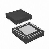
ATMEGA48V-10MMU Atmel, ATMEGA48V-10MMU Datasheet - Page 283

ATMEGA48V-10MMU
Manufacturer Part Number
ATMEGA48V-10MMU
Description
MCU AVR 4K FLASH 10MHZ 28-QFN
Manufacturer
Atmel
Series
AVR® ATmegar
Specifications of ATMEGA48V-10MMU
Core Processor
AVR
Core Size
8-Bit
Speed
10MHz
Connectivity
I²C, SPI, UART/USART
Peripherals
Brown-out Detect/Reset, POR, PWM, WDT
Number Of I /o
23
Program Memory Size
4KB (2K x 16)
Program Memory Type
FLASH
Eeprom Size
256 x 8
Ram Size
512 x 8
Voltage - Supply (vcc/vdd)
1.8 V ~ 5.5 V
Data Converters
A/D 8x10b
Oscillator Type
Internal
Operating Temperature
-40°C ~ 85°C
Package / Case
28-VQFN Exposed Pad, 28-HVQFN, 28-SQFN, 28-DHVQFN
Processor Series
ATMEGA48x
Core
AVR8
Data Bus Width
8 bit
Data Ram Size
512 B
Interface Type
2-Wire, SPI, USART, Serial
Maximum Clock Frequency
10 MHz
Number Of Programmable I/os
23
Number Of Timers
3
Maximum Operating Temperature
+ 85 C
Mounting Style
SMD/SMT
3rd Party Development Tools
EWAVR, EWAVR-BL
Minimum Operating Temperature
- 40 C
On-chip Adc
10 bit, 8 Channel
Package
28MLF EP
Device Core
AVR
Family Name
ATmega
Maximum Speed
10 MHz
Operating Supply Voltage
2.5|3.3|5 V
For Use With
ATSTK600 - DEV KIT FOR AVR/AVR32ATAVRDRAGON - KIT DRAGON 32KB FLASH MEM AVR
Lead Free Status / RoHS Status
Lead free / RoHS Compliant
Available stocks
Company
Part Number
Manufacturer
Quantity
Price
Company:
Part Number:
ATMEGA48V-10MMU
Manufacturer:
ZILOG
Quantity:
1
- Current page: 283 of 378
- Download datasheet (8Mb)
ATmega48/88/168
• Bit 5 – Res: Reserved Bit
This bit is a reserved bit in the ATmega48/88/168 and always read as zero.
• Bit 4 – RWWSRE: Read-While-Write Section Read Enable
When programming (Page Erase or Page Write) to the RWW section, the RWW section is
blocked for reading (the RWWSB will be set by hardware). To re-enable the RWW section, the
user software must wait until the programming is completed (SELFPRGEN will be cleared).
Then, if the RWWSRE bit is written to one at the same time as SELFPRGEN, the next SPM
instruction within four clock cycles re-enables the RWW section. The RWW section cannot be
re-enabled while the Flash is busy with a Page Erase or a Page Write (SELFPRGEN is set). If
the RWWSRE bit is written while the Flash is being loaded, the Flash load operation will abort
and the data loaded will be lost.
• Bit 3 – BLBSET: Boot Lock Bit Set
If this bit is written to one at the same time as SELFPRGEN, the next SPM instruction within four
clock cycles sets Boot Lock bits and Memory Lock bits, according to the data in R0. The data in
R1 and the address in the Z-pointer are ignored. The BLBSET bit will automatically be cleared
upon completion of the Lock bit set, or if no SPM instruction is executed within four clock cycles.
An LPM instruction within three cycles after BLBSET and SELFPRGEN are set in the SPMCSR
Register, will read either the Lock bits or the Fuse bits (depending on Z0 in the Z-pointer) into the
destination register. See
“Reading the Fuse and Lock Bits from Software” on page 276
for
details.
• Bit 2 – PGWRT: Page Write
If this bit is written to one at the same time as SELFPRGEN, the next SPM instruction within four
clock cycles executes Page Write, with the data stored in the temporary buffer. The page
address is taken from the high part of the Z-pointer. The data in R1 and R0 are ignored. The
PGWRT bit will auto-clear upon completion of a Page Write, or if no SPM instruction is executed
within four clock cycles. The CPU is halted during the entire Page Write operation if the NRWW
section is addressed.
• Bit 1 – PGERS: Page Erase
If this bit is written to one at the same time as SELFPRGEN, the next SPM instruction within four
clock cycles executes Page Erase. The page address is taken from the high part of the Z-
pointer. The data in R1 and R0 are ignored. The PGERS bit will auto-clear upon completion of a
Page Erase, or if no SPM instruction is executed within four clock cycles. The CPU is halted dur-
ing the entire Page Write operation if the NRWW section is addressed.
• Bit 0 – SELFPRGEN: Self Programming Enable
This bit enables the SPM instruction for the next four clock cycles. If written to one together with
either RWWSRE, BLBSET, PGWRT or PGERS, the following SPM instruction will have a spe-
cial meaning, see description above. If only SELFPRGEN is written, the following SPM
instruction will store the value in R1:R0 in the temporary page buffer addressed by the Z-pointer.
The LSB of the Z-pointer is ignored. The SELFPRGEN bit will auto-clear upon completion of an
SPM instruction, or if no SPM instruction is executed within four clock cycles. During Page Erase
and Page Write, the SELFPRGEN bit remains high until the operation is completed.
Writing any other combination than “10001”, “01001”, “00101”, “00011” or “00001” in the lower
five bits will have no effect.
283
2545S–AVR–07/10
Related parts for ATMEGA48V-10MMU
Image
Part Number
Description
Manufacturer
Datasheet
Request
R

Part Number:
Description:
IC AVR MCU 4K 5V 10MHZ 32-TQFP
Manufacturer:
Atmel
Datasheet:

Part Number:
Description:
IC AVR MCU 4K 10MHZ 1.8V 32-QFN
Manufacturer:
Atmel
Datasheet:

Part Number:
Description:
IC AVR MCU 4K 10MHZ 1.8V 28DIP
Manufacturer:
Atmel
Datasheet:

Part Number:
Description:
IC AVR MCU 4K 5V 10MHZ 32-TQFP
Manufacturer:
Atmel
Datasheet:

Part Number:
Description:
IC AVR MCU 4K 5V 12MHZ 32-QFN
Manufacturer:
Atmel
Datasheet:

Part Number:
Description:
IC AVR MCU 4K 5V 10MHZ 32-QFN
Manufacturer:
Atmel
Datasheet:

Part Number:
Description:
IC AVR MCU 4K 5V 10MHZ 28-DIP
Manufacturer:
Atmel
Datasheet:

Part Number:
Description:
IC AVR MCU 4K 5V 10MHZ 28-DIP
Manufacturer:
Atmel
Datasheet:

Part Number:
Description:
MCU AVR 4KB FLASH 10MHZ 32TQFP
Manufacturer:
Atmel
Datasheet:

Part Number:
Description:
MCU AVR 4KB FLASH 10MHZ 32QFN
Manufacturer:
Atmel
Datasheet:

Part Number:
Description:
MCU AVR 4KB FLASH 20MHZ 28QFN
Manufacturer:
Atmel
Datasheet:


