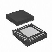
ATMEGA48V-10MMU Atmel, ATMEGA48V-10MMU Datasheet - Page 308

ATMEGA48V-10MMU
Manufacturer Part Number
ATMEGA48V-10MMU
Description
MCU AVR 4K FLASH 10MHZ 28-QFN
Manufacturer
Atmel
Series
AVR® ATmegar
Specifications of ATMEGA48V-10MMU
Core Processor
AVR
Core Size
8-Bit
Speed
10MHz
Connectivity
I²C, SPI, UART/USART
Peripherals
Brown-out Detect/Reset, POR, PWM, WDT
Number Of I /o
23
Program Memory Size
4KB (2K x 16)
Program Memory Type
FLASH
Eeprom Size
256 x 8
Ram Size
512 x 8
Voltage - Supply (vcc/vdd)
1.8 V ~ 5.5 V
Data Converters
A/D 8x10b
Oscillator Type
Internal
Operating Temperature
-40°C ~ 85°C
Package / Case
28-VQFN Exposed Pad, 28-HVQFN, 28-SQFN, 28-DHVQFN
Processor Series
ATMEGA48x
Core
AVR8
Data Bus Width
8 bit
Data Ram Size
512 B
Interface Type
2-Wire, SPI, USART, Serial
Maximum Clock Frequency
10 MHz
Number Of Programmable I/os
23
Number Of Timers
3
Maximum Operating Temperature
+ 85 C
Mounting Style
SMD/SMT
3rd Party Development Tools
EWAVR, EWAVR-BL
Minimum Operating Temperature
- 40 C
On-chip Adc
10 bit, 8 Channel
Package
28MLF EP
Device Core
AVR
Family Name
ATmega
Maximum Speed
10 MHz
Operating Supply Voltage
2.5|3.3|5 V
For Use With
ATSTK600 - DEV KIT FOR AVR/AVR32ATAVRDRAGON - KIT DRAGON 32KB FLASH MEM AVR
Lead Free Status / RoHS Status
Lead free / RoHS Compliant
Available stocks
Company
Part Number
Manufacturer
Quantity
Price
Company:
Part Number:
ATMEGA48V-10MMU
Manufacturer:
ZILOG
Quantity:
1
- Current page: 308 of 378
- Download datasheet (8Mb)
28.7
308
3. C
4. f
5. This requirement applies to all ATmega48/88/168 2-wire Serial Interface operation. Other devices connected to the 2-wire
SPI Timing Characteristics
ATmega48/88/168
Serial Bus need only obey the general f
CK
b
= capacitance of one bus line in pF.
= CPU clock frequency
Figure 28-4. 2-wire Serial Bus Timing
See
Table 28-6.
Note:
SCL
SDA
1
2
3
4
5
6
7
8
9
10
11
12
13
14
15
16
17
18
Figure 28-5
t
SU;STA
Description
SCK period
SCK high/low
Rise/Fall time
Setup
Hold
Out to SCK
SCK to out
SCK to out high
SS low to out
SCK period
SCK high/low
Rise/Fall time
Setup
Hold
SCK to out
SCK to SS high
SS high to tri-state
SS low to SCK
1. In SPI Programming mode the minimum SCK high/low period is:
- 2 t
- 3 t
SPI Timing Parameters
CLCL
CLCL
and
for f
for f
(1)
SCL
Figure 28-6
CK
CK
requirement.
t
HD;STA
< 12 MHz
> 12 MHz
t
t
of
LOW
Master
Master
Master
Master
Master
Master
Master
Slave
Slave
Slave
Slave
Slave
Slave
Slave
Slave
Mode
Master
Slave
Slave
for details.
t
HIGH
t
HD;DAT
Min
4 • t
2 • t
10
t
20
20
ck
ck
ck
t
LOW
t
SU;DAT
Typ
See
50% duty cycle
3.6
10
10
0.5 • t
10
10
15
15
10
Table 18-5
sck
Max
1600
t
SU;STO
t
r
2545S–AVR–07/10
t
BUF
ns
Related parts for ATMEGA48V-10MMU
Image
Part Number
Description
Manufacturer
Datasheet
Request
R

Part Number:
Description:
IC AVR MCU 4K 5V 10MHZ 32-TQFP
Manufacturer:
Atmel
Datasheet:

Part Number:
Description:
IC AVR MCU 4K 10MHZ 1.8V 32-QFN
Manufacturer:
Atmel
Datasheet:

Part Number:
Description:
IC AVR MCU 4K 10MHZ 1.8V 28DIP
Manufacturer:
Atmel
Datasheet:

Part Number:
Description:
IC AVR MCU 4K 5V 10MHZ 32-TQFP
Manufacturer:
Atmel
Datasheet:

Part Number:
Description:
IC AVR MCU 4K 5V 12MHZ 32-QFN
Manufacturer:
Atmel
Datasheet:

Part Number:
Description:
IC AVR MCU 4K 5V 10MHZ 32-QFN
Manufacturer:
Atmel
Datasheet:

Part Number:
Description:
IC AVR MCU 4K 5V 10MHZ 28-DIP
Manufacturer:
Atmel
Datasheet:

Part Number:
Description:
IC AVR MCU 4K 5V 10MHZ 28-DIP
Manufacturer:
Atmel
Datasheet:

Part Number:
Description:
MCU AVR 4KB FLASH 10MHZ 32TQFP
Manufacturer:
Atmel
Datasheet:

Part Number:
Description:
MCU AVR 4KB FLASH 10MHZ 32QFN
Manufacturer:
Atmel
Datasheet:

Part Number:
Description:
MCU AVR 4KB FLASH 20MHZ 28QFN
Manufacturer:
Atmel
Datasheet:


