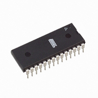
ATMEGA48PA-PU Atmel, ATMEGA48PA-PU Datasheet - Page 314

ATMEGA48PA-PU
Manufacturer Part Number
ATMEGA48PA-PU
Description
MCU AVR 4KB FLASH IND 28PDIP
Manufacturer
Atmel
Series
AVR® ATmegar
Specifications of ATMEGA48PA-PU
Core Processor
AVR
Core Size
8-Bit
Speed
20MHz
Connectivity
I²C, SPI, UART/USART
Peripherals
Brown-out Detect/Reset, POR, PWM, WDT
Number Of I /o
23
Program Memory Size
4KB (2K x 16)
Program Memory Type
FLASH
Eeprom Size
256 x 8
Ram Size
512 x 8
Voltage - Supply (vcc/vdd)
1.8 V ~ 5.5 V
Data Converters
A/D 6x10b
Oscillator Type
Internal
Operating Temperature
-40°C ~ 85°C
Package / Case
28-DIP (0.300", 7.62mm)
Processor Series
ATMEGA48x
Core
AVR8
Data Bus Width
8 bit
Data Ram Size
512 B
Interface Type
2-Wire, SPI, USART
Maximum Clock Frequency
20 MHz
Number Of Programmable I/os
23
Number Of Timers
3
Maximum Operating Temperature
+ 85 C
Mounting Style
Through Hole
3rd Party Development Tools
EWAVR, EWAVR-BL
Development Tools By Supplier
ATAVRDRAGON, ATSTK500, ATSTK600, ATAVRISP2, ATAVRONEKIT
Minimum Operating Temperature
- 40 C
On-chip Adc
10 bit, 6 Channel
On-chip Dac
10 bit, 6 Channel
For Use With
ATSTK600 - DEV KIT FOR AVR/AVR32ATAVRDRAGON - KIT DRAGON 32KB FLASH MEM AVR
Lead Free Status / RoHS Status
Lead free / RoHS Compliant
Available stocks
Company
Part Number
Manufacturer
Quantity
Price
Company:
Part Number:
ATMEGA48PA-PU
Manufacturer:
ON
Quantity:
21 000
- Current page: 314 of 566
- Download datasheet (23Mb)
Table 27-19. Serial Programming Instruction Set (Hexadecimal values) (Continued)
Notes:
8271C–AVR–08/10
Instruction/Operation
Read Calibration Byte
Write Instructions
Write Program Memory Page
Write EEPROM Memory
Write EEPROM Memory Page (page access)
Write Lock bits
Write Fuse bits
Write Fuse High bits
Write Extended Fuse Bits
1. Not all instructions are applicable for all parts.
2. a = address.
3. Bits are programmed ‘0’, unprogrammed ‘1’.
4. To ensure future compatibility, unused Fuses and Lock bits should be unprogrammed (‘1’) .
5. Refer to the corresponding section for Fuse and Lock bits, Calibration and Signature bytes and Page size.
6. Instructions accessing program memory use a word address. This address may be random within the page range.
7. See http://www.atmel.com/avr for Application Notes regarding programming and programmers.
8. WORDS
(6)
If the LSB in RDY/BSY data byte out is ‘1’, a programming operation is still pending. Wait until
this bit returns ‘0’ before the next instruction is carried out.
Within the same page, the low data byte must be loaded prior to the high data byte.
After data is loaded to the page buffer, program the EEPROM page, see
315.
ATmega48A/48PA/88A/88PA/168A/168PA/328/328
Byte 1
$AC
$AC
$AC
$AC
$4C
$C0
$C2
$38
adr MSB
0000 00aa
0000 00aa
Byte 2
$E0
$A0
$A8
$A4
$00
Instruction Format
(8)
aaaa aaaa
aaaa aa00
adr LSB
Byte 3
$00
$00
$00
$00
$00
(8)
Figure 27-8 on page
data byte out
data byte in
data byte in
data byte in
data byte in
data byte in
Byte4
$00
$00
314
Related parts for ATMEGA48PA-PU
Image
Part Number
Description
Manufacturer
Datasheet
Request
R

Part Number:
Description:
IC AVR MCU 4K 5V 20MHZ 32-TQFP
Manufacturer:
Atmel
Datasheet:

Part Number:
Description:
Manufacturer:
Atmel Corporation
Datasheet:

Part Number:
Description:
Manufacturer:
Atmel Corporation
Datasheet:

Part Number:
Description:
IC AVR MCU 4K 20MHZ 5V 32TQFP
Manufacturer:
Atmel
Datasheet:

Part Number:
Description:
IC AVR MCU 4K 20MHZ 5V 28DIP
Manufacturer:
Atmel
Datasheet:

Part Number:
Description:
IC AVR MCU 4K 20MHZ 5V 32-QFN
Manufacturer:
Atmel
Datasheet:

Part Number:
Description:
IC AVR MCU 4K 5V 20MHZ 32-TQFP
Manufacturer:
Atmel
Datasheet:

Part Number:
Description:
IC AVR MCU 4K 5V 20MHZ 32-QFN
Manufacturer:
Atmel
Datasheet:

Part Number:
Description:
IC AVR MCU 4K 5V 20MHZ 32-QFN
Manufacturer:
Atmel
Datasheet:

Part Number:
Description:
IC AVR MCU 4K 5V 20MHZ 28-DIP
Manufacturer:
Atmel
Datasheet:

Part Number:
Description:
IC AVR MCU 4K 5V 20MHZ 28-DIP
Manufacturer:
Atmel
Datasheet:

Part Number:
Description:
IC AVR MCU 4K FLASH 20MHZ 28QFN
Manufacturer:
Atmel
Datasheet:


