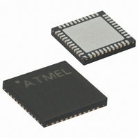
ATMEGA16-16MQ Atmel, ATMEGA16-16MQ Datasheet - Page 75

ATMEGA16-16MQ
Manufacturer Part Number
ATMEGA16-16MQ
Description
MCU AVR 16K FLASH 16MHZ 44-QFN
Manufacturer
Atmel
Series
AVR® ATmegar
Datasheet
1.ATMEGA16L-8MI.pdf
(357 pages)
Specifications of ATMEGA16-16MQ
Core Processor
AVR
Core Size
8-Bit
Speed
16MHz
Connectivity
I²C, SPI, UART/USART
Peripherals
Brown-out Detect/Reset, POR, PWM, WDT
Number Of I /o
32
Program Memory Size
16KB (8K x 16)
Program Memory Type
FLASH
Eeprom Size
512 x 8
Ram Size
1K x 8
Voltage - Supply (vcc/vdd)
4.5 V ~ 5.5 V
Data Converters
A/D 8x10b
Oscillator Type
Internal
Operating Temperature
-40°C ~ 85°C
Package / Case
44-VQFN Exposed Pad
Processor Series
ATMEGA16x
Core
AVR8
Data Bus Width
8 bit
Data Ram Size
1 KB
Mounting Style
SMD/SMT
3rd Party Development Tools
EWAVR, EWAVR-BL
Development Tools By Supplier
ATAVRDRAGON, ATSTK500, ATSTK600, ATAVRISP2, ATAVRONEKIT
For Use With
ATSTK600-TQFP44 - STK600 SOCKET/ADAPTER 44-TQFPATSTK500 - PROGRAMMER AVR STARTER KIT
Lead Free Status / RoHS Status
Lead free / RoHS Compliant
- Current page: 75 of 357
- Download datasheet (8Mb)
Compare Output Mode
and Waveform
Generation
2466T–AVR–07/10
Figure 30. Compare Match Output Unit, Schematic
The general I/O port function is overridden by the Output Compare (OC0) from the Waveform
Generator if either of the COM01:0 bits are set. However, the OC0 pin direction (input or output)
is still controlled by the Data Direction Register (DDR) for the port pin. The Data Direction Regis-
ter bit for the OC0 pin (DDR_OC0) must be set as output before the OC0 value is visible on the
pin. The port override function is independent of the Waveform Generation mode.
The design of the output compare pin logic allows initialization of the OC0 state before the out-
put is enabled. Note that some COM01:0 bit settings are reserved for certain modes of
operation.
The Waveform Generator uses the COM01:0 bits differently in normal, CTC, and PWM modes.
For all modes, setting the COM01:0 = 0 tells the waveform generator that no action on the OC0
Register is to be performed on the next compare match. For compare output actions in the non-
PWM modes refer to
and for phase correct PWM refer to
A change of the COM01:0 bits state will have effect at the first compare match after the bits are
written. For non-PWM modes, the action can be forced to have immediate effect by using the
FOC0 strobe bits.
See “8-bit Timer/Counter Register Description” on page 83.
COMn1
COMn0
FOCn
clk
I/O
Table 39 on page
Waveform
Generator
Table 41 on page
84. For fast PWM mode, refer to
D
D
D
PORT
DDR
OCn
Q
Q
Q
84.
1
0
ATmega16(L)
Table 40 on page
OCn
Pin
84,
75
Related parts for ATMEGA16-16MQ
Image
Part Number
Description
Manufacturer
Datasheet
Request
R

Part Number:
Description:
Manufacturer:
Atmel Corporation
Datasheet:

Part Number:
Description:
IC AVR MCU 16K 16MHZ 5V 44TQFP
Manufacturer:
Atmel
Datasheet:

Part Number:
Description:
IC AVR MCU 16K 16MHZ 5V 44-QFN
Manufacturer:
Atmel
Datasheet:

Part Number:
Description:
IC AVR MCU 16K 16MHZ 5V 40DIP
Manufacturer:
Atmel
Datasheet:

Part Number:
Description:
IC AVR MCU 16K 16MHZ COM 40-DIP
Manufacturer:
Atmel
Datasheet:

Part Number:
Description:
IC AVR MCU 16K 16MHZ COM 44-QFN
Manufacturer:
Atmel
Datasheet:

Part Number:
Description:
IC AVR MCU 16K 16MHZ IND 40-DIP
Manufacturer:
Atmel
Datasheet:

Part Number:
Description:
IC AVR MCU 16K 16MHZ IND 44-QFN
Manufacturer:
Atmel
Datasheet:

Part Number:
Description:
IC AVR MCU 16K 16MHZ IND 44-TQFP
Manufacturer:
Atmel
Datasheet:

Part Number:
Description:
IC MCU 8BIT 16KB FLASH 44TQFP
Manufacturer:
Atmel
Datasheet:

Part Number:
Description:
MCU AVR 16K FLASH 16MHZ 44-TQFP
Manufacturer:
Atmel
Datasheet:

Part Number:
Description:
IC AVR MCU 16K 16MHZ COM 44-TQFP
Manufacturer:
Atmel
Datasheet:

Part Number:
Description:
IC MCU AVR 16K 5V 16MHZ 44-TQFP
Manufacturer:
Atmel
Datasheet:


