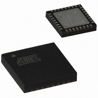
AT89C5131A-PUTUM Atmel, AT89C5131A-PUTUM Datasheet - Page 10

AT89C5131A-PUTUM
Manufacturer Part Number
AT89C5131A-PUTUM
Description
IC 8051 MCU FLASH 32K USB 32QFN
Manufacturer
Atmel
Series
AT89C513xr
Datasheet
1.AT89C5130A-PUTUM.pdf
(188 pages)
Specifications of AT89C5131A-PUTUM
Core Processor
C52X2
Core Size
8-Bit
Speed
48MHz
Connectivity
I²C, SPI, UART/USART, USB
Peripherals
LED, POR, PWM, WDT
Number Of I /o
18
Program Memory Size
32KB (32K x 8)
Program Memory Type
FLASH
Eeprom Size
4K x 8
Ram Size
1.25K x 8
Voltage - Supply (vcc/vdd)
2.7 V ~ 5.5 V
Oscillator Type
Internal
Operating Temperature
-40°C ~ 85°C
Package / Case
32-VQFN Exposed Pad, 32-HVQFN, 32-SQFN, 32-DHVQFN
Core
8051
Processor Series
AT89x
Data Bus Width
8 bit
Maximum Clock Frequency
48 MHz
Data Ram Size
1.25 KB
Number Of Programmable I/os
34
Number Of Timers
16 bit
Operating Supply Voltage
2.7 V to 5.5 V
Mounting Style
SMD/SMT
Height
0.95 mm
Interface Type
2-Wire, EUART, SPI, USB
Length
7 mm
Maximum Operating Temperature
+ 85 C
Minimum Operating Temperature
- 40 C
Supply Voltage (max)
5.5 V
Supply Voltage (min)
2.7 V
Width
7 mm
For Use With
AT89OCD-01 - USB EMULATOR FOR AT8XC51 MCUAT89STK-10 - KIT EVAL APPL MASS STORAGEAT89STK-05 - KIT STARTER FOR AT89C5131
Lead Free Status / RoHS Status
Lead free / RoHS Compliant
Data Converters
-
Lead Free Status / Rohs Status
Details
Available stocks
Company
Part Number
Manufacturer
Quantity
Price
Part Number:
AT89C5131A-PUTUM
Manufacturer:
ATMEL/爱特梅尔
Quantity:
20 000
10
AT89C5130A/31A-M
Table 3-10.
Table 3-11.
Table 3-12.
AD[7:0]
Signal
Signal
A[15:8]
Signal
Name
Name
PSEN
Name
VREF
AVSS
RST
ALE
WR
RD
D+
EA
D-
USB Signal Description
System Signal Description
Power Signal Description
Type
Type
Type
GND
I/O
I/O
I/O
I/O
I/O
I/O
I/O
O
O
O
I
Description
USB Data + signal
Set to high level under reset.
USB Data - signal
Set to low level under reset.
USB Reference Voltage
Connect this pin to D+ using a 1.5 kΩ resistor to use the Detach function.
Description
Multiplexed Address/Data LSB for external access
Data LSB for Slave port access (used for 8-bit and 16-bit modes)
Address Bus MSB for external access
Read Signal
Read signal asserted during external data memory read operation.
Control input for slave port read access cycles.
Write Signal
Write signal asserted during external data memory write operation.
Control input for slave write access cycles.
Reset Input
Holding this pin low for 64 oscillator periods while the oscillator is running
resets the device. The Port pins are driven to their reset conditions when a
voltage lower than V
This pin has an internal pull-up resistor which allows the device to be reset
by connecting a capacitor between this pin and VSS.
Asserting RST when the chip is in Idle mode or Power-down mode returns
the chip to normal operation.
This pin is tied to 0 for at least 12 oscillator periods when an internal reset
occurs ( hardware watchdog or power monitor).
Address Latch Enable Output
The falling edge of ALE strobes the address into external latch. This signal
is active only when reading or writing external memory using MOVX
instructions.
Program Strobe Enable / Hardware conditions Input for ISP
Used as input under reset to detect external hardware conditions of ISP
mode.
External Access Enable
This pin must be held low to force the device to fetch code from external
program memory starting at address 0000h.
Description
Analog Ground
AVSS is used to supply the on-chip PLL and the USB PAD.
IL
is applied, whether or not the oscillator is running.
4337K–USB–04/08
Alternate
Alternate
Alternate
Function
Function
Function
P0[7:0]
P2[7:0]
P3.7
P3.6
-
-
-
-
-
-
-
-


