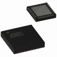
AT89C5131A-PUTUM Atmel, AT89C5131A-PUTUM Datasheet - Page 127

AT89C5131A-PUTUM
Manufacturer Part Number
AT89C5131A-PUTUM
Description
IC 8051 MCU FLASH 32K USB 32QFN
Manufacturer
Atmel
Series
AT89C513xr
Datasheet
1.AT89C5130A-PUTUM.pdf
(188 pages)
Specifications of AT89C5131A-PUTUM
Core Processor
C52X2
Core Size
8-Bit
Speed
48MHz
Connectivity
I²C, SPI, UART/USART, USB
Peripherals
LED, POR, PWM, WDT
Number Of I /o
18
Program Memory Size
32KB (32K x 8)
Program Memory Type
FLASH
Eeprom Size
4K x 8
Ram Size
1.25K x 8
Voltage - Supply (vcc/vdd)
2.7 V ~ 5.5 V
Oscillator Type
Internal
Operating Temperature
-40°C ~ 85°C
Package / Case
32-VQFN Exposed Pad, 32-HVQFN, 32-SQFN, 32-DHVQFN
Core
8051
Processor Series
AT89x
Data Bus Width
8 bit
Maximum Clock Frequency
48 MHz
Data Ram Size
1.25 KB
Number Of Programmable I/os
34
Number Of Timers
16 bit
Operating Supply Voltage
2.7 V to 5.5 V
Mounting Style
SMD/SMT
Height
0.95 mm
Interface Type
2-Wire, EUART, SPI, USB
Length
7 mm
Maximum Operating Temperature
+ 85 C
Minimum Operating Temperature
- 40 C
Supply Voltage (max)
5.5 V
Supply Voltage (min)
2.7 V
Width
7 mm
For Use With
AT89OCD-01 - USB EMULATOR FOR AT8XC51 MCUAT89STK-10 - KIT EVAL APPL MASS STORAGEAT89STK-05 - KIT STARTER FOR AT89C5131
Lead Free Status / RoHS Status
Lead free / RoHS Compliant
Data Converters
-
Lead Free Status / Rohs Status
Details
Available stocks
Company
Part Number
Manufacturer
Quantity
Price
Part Number:
AT89C5131A-PUTUM
Manufacturer:
ATMEL/爱特梅尔
Quantity:
20 000
21.4.2
4337K–USB–04/08
Bulk/Interrupt OUT Transactions in Ping-pong Mode
Figure 21-8. Bulk/Interrupt OUT Transactions in Ping-pong Mode
An endpoint will be first enabled and configured before being able to receive Bulk or Interrupt
packets.
When a valid OUT packet is received on the endpoint bank 0, the RXOUTB0 bit is set by the
USB controller. This triggers an interrupt if enabled. The firmware has to select the correspond-
ing endpoint, store the number of data bytes by reading the UBYCTLX and UBYCTHX registers.
If the received packet is a ZLP (Zero Length Packet), the UBYCTLX and UBYCTHX register val-
ues are equal to 0 and no data has to be read.
When all the endpoint FIFO bytes have been read, the firmware will clear the RXOUB0 bit to
allow the USB controller to accept the next OUT packet on the endpoint bank 0. This action
switches the endpoint bank 0 and 1. Until the RXOUTB0 bit has been cleared by the firmware,
the USB controller will answer a NAK handshake for each OUT requests on the bank 0 endpoint
FIFO.
When a new valid OUT packet is received on the endpoint bank 1, the RXOUTB1 bit is set by
the USB controller. This triggers an interrupt if enabled. The firmware empties the bank 1 end-
point FIFO before clearing the RXOUTB1 bit. Until the RXOUTB1 bit has been cleared by the
firmware, the USB controller will answer a NAK handshake for each OUT requests on the bank 1
endpoint FIFO.
The RXOUTB0 and RXOUTB1 bits are alternatively set by the USB controller at each new valid
packet receipt.
The firmware has to clear one of these two bits after having read all the data FIFO to allow a new
valid packet to be stored in the corresponding bank.
OUT
OUT
OUT
HOST
DATA0 (n Bytes)
DATA1 (m Bytes)
DATA0 (p Bytes)
ACK
ACK
ACK
UFI
RXOUTB0
RXOUTB1
RXOUTB0
Endpoint FIFO Bank 0 - Read Byte 1
Endpoint FIFO Bank 0 - Read Byte 2
Endpoint FIFO Bank 0 - Read Byte n
Endpoint FIFO Bank 1 - Read Byte 1
Endpoint FIFO Bank 1 - Read Byte 2
Endpoint FIFO Bank 1 - Read Byte m
Endpoint FIFO Bank 0 - Read Byte 1
Endpoint FIFO Bank 0 - Read Byte 2
Endpoint FIFO Bank 0 - Read Byte p
AT89C5130A/31A-M
Clear RXOUTB0
Clear RXOUTB1
Clear RXOUTB0
C51
127


