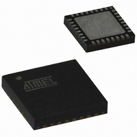
AT89C5131A-PUTUM Atmel, AT89C5131A-PUTUM Datasheet - Page 29

AT89C5131A-PUTUM
Manufacturer Part Number
AT89C5131A-PUTUM
Description
IC 8051 MCU FLASH 32K USB 32QFN
Manufacturer
Atmel
Series
AT89C513xr
Datasheet
1.AT89C5130A-PUTUM.pdf
(188 pages)
Specifications of AT89C5131A-PUTUM
Core Processor
C52X2
Core Size
8-Bit
Speed
48MHz
Connectivity
I²C, SPI, UART/USART, USB
Peripherals
LED, POR, PWM, WDT
Number Of I /o
18
Program Memory Size
32KB (32K x 8)
Program Memory Type
FLASH
Eeprom Size
4K x 8
Ram Size
1.25K x 8
Voltage - Supply (vcc/vdd)
2.7 V ~ 5.5 V
Oscillator Type
Internal
Operating Temperature
-40°C ~ 85°C
Package / Case
32-VQFN Exposed Pad, 32-HVQFN, 32-SQFN, 32-DHVQFN
Core
8051
Processor Series
AT89x
Data Bus Width
8 bit
Maximum Clock Frequency
48 MHz
Data Ram Size
1.25 KB
Number Of Programmable I/os
34
Number Of Timers
16 bit
Operating Supply Voltage
2.7 V to 5.5 V
Mounting Style
SMD/SMT
Height
0.95 mm
Interface Type
2-Wire, EUART, SPI, USB
Length
7 mm
Maximum Operating Temperature
+ 85 C
Minimum Operating Temperature
- 40 C
Supply Voltage (max)
5.5 V
Supply Voltage (min)
2.7 V
Width
7 mm
For Use With
AT89OCD-01 - USB EMULATOR FOR AT8XC51 MCUAT89STK-10 - KIT EVAL APPL MASS STORAGEAT89STK-05 - KIT STARTER FOR AT89C5131
Lead Free Status / RoHS Status
Lead free / RoHS Compliant
Data Converters
-
Lead Free Status / Rohs Status
Details
Available stocks
Company
Part Number
Manufacturer
Quantity
Price
Part Number:
AT89C5131A-PUTUM
Manufacturer:
ATMEL/爱特梅尔
Quantity:
20 000
- Current page: 29 of 188
- Download datasheet (2Mb)
8. Program/Code Memory
8.1
8.1.1
4337K–USB–04/08
External Code Memory Access
Memory Interface
The AT89C5130A/31A-M implement 16/ 32 Kbytes of on-chip program/code memory. Figure 8-
1 shows the split of internal and external program/code memory spaces depending on the
product.
The Flash memory increases EPROM and ROM functionality by in-circuit electrical erasure and
programming. Thanks to the internal charge pump, the high voltage needed for programming or
erasing Flash cells is generated on-chip using the standard V
ory can be programmed using only one voltage and allows In- application Software
Programming commonly known as IAP. Hardware programming mode is also available using
specific programming tool.
Figure 8-1.
Note:
The external memory interface comprises the external bus (Port 0 and Port 2) as well as the bus
control signals (PSEN, and ALE).
Figure 8-2 shows the structure of the external address bus. P0 carries address A7:0 while P2
carries address A15:8. Data D7:0 is multiplexed with A7:0 on P0. Table 8-1 describes the exter-
nal memory interface signals.
If the program executes exclusively from on-chip code memory (not from external memory),
beware of executing code from the upper byte of on-chip memory (3FFFh/7FFFh) and thereby
disrupting I/O Ports 0 and 2 due to external prefetch. Fetching code constant from this location
does not affect Ports 0 and 2.
FFFFh
3FFFh
4000h
0000h
Program/Code Memory Organization
AT89C5130A
External Code
48 Kbytes
16 Kbytes
Flash
AT89C5130A/31A-M
DD
FFFFh
7FFFh
8000h
0000h
voltage. Thus, the Flash Mem-
AT89C5131A
External Code
32 Kbytes
32 Kbytes
Flash
29
Related parts for AT89C5131A-PUTUM
Image
Part Number
Description
Manufacturer
Datasheet
Request
R

Part Number:
Description:
Manufacturer:
Atmel Corporation
Datasheet:

Part Number:
Description:
Manufacturer:
Atmel Corporation
Datasheet:

Part Number:
Description:
IC 8051 MCU FLASH 32K USB 52PLCC
Manufacturer:
Atmel
Datasheet:

Part Number:
Description:
IC MCU 32KB 3-3.6V USB 48-VQFN
Manufacturer:
Atmel
Datasheet:

Part Number:
Description:
MCU 8051 32K FLASH USB 28-SOIC
Manufacturer:
Atmel
Datasheet:

Part Number:
Description:
IC 8051 MCU FLASH 32K USB 64VQFP
Manufacturer:
Atmel
Datasheet:

Part Number:
Description:
MCU 8051 32K FLASH USB 64-VQFP
Manufacturer:
Atmel
Datasheet:

Part Number:
Description:
MCU 8051 32K FLASH USB 28-SOIC
Manufacturer:
Atmel
Datasheet:

Part Number:
Description:
MCU 8051 32K FLASH USB 52-PLCC
Manufacturer:
Atmel
Datasheet:

Part Number:
Description:
IC 8051 MCU FLASH 32K USB 48QFN
Manufacturer:
Atmel
Datasheet:

Part Number:
Description:
IC 8051 MCU FLASH 32K USB 64VQFP
Manufacturer:
Atmel
Datasheet:

Part Number:
Description:
IC 8051 MCU FLASH 32K USB 32QFN
Manufacturer:
Atmel
Datasheet:

Part Number:
Description:
IC 8051 MCU FLASH 32K USB 52PLCC
Manufacturer:
Atmel
Datasheet:

Part Number:
Description:
IC 8051 MCU FLASH 32K USB 28SOIC
Manufacturer:
Atmel
Datasheet:


