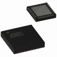
AT89C5131A-PUTUM Atmel, AT89C5131A-PUTUM Datasheet - Page 7

AT89C5131A-PUTUM
Manufacturer Part Number
AT89C5131A-PUTUM
Description
IC 8051 MCU FLASH 32K USB 32QFN
Manufacturer
Atmel
Series
AT89C513xr
Datasheet
1.AT89C5130A-PUTUM.pdf
(188 pages)
Specifications of AT89C5131A-PUTUM
Core Processor
C52X2
Core Size
8-Bit
Speed
48MHz
Connectivity
I²C, SPI, UART/USART, USB
Peripherals
LED, POR, PWM, WDT
Number Of I /o
18
Program Memory Size
32KB (32K x 8)
Program Memory Type
FLASH
Eeprom Size
4K x 8
Ram Size
1.25K x 8
Voltage - Supply (vcc/vdd)
2.7 V ~ 5.5 V
Oscillator Type
Internal
Operating Temperature
-40°C ~ 85°C
Package / Case
32-VQFN Exposed Pad, 32-HVQFN, 32-SQFN, 32-DHVQFN
Core
8051
Processor Series
AT89x
Data Bus Width
8 bit
Maximum Clock Frequency
48 MHz
Data Ram Size
1.25 KB
Number Of Programmable I/os
34
Number Of Timers
16 bit
Operating Supply Voltage
2.7 V to 5.5 V
Mounting Style
SMD/SMT
Height
0.95 mm
Interface Type
2-Wire, EUART, SPI, USB
Length
7 mm
Maximum Operating Temperature
+ 85 C
Minimum Operating Temperature
- 40 C
Supply Voltage (max)
5.5 V
Supply Voltage (min)
2.7 V
Width
7 mm
For Use With
AT89OCD-01 - USB EMULATOR FOR AT8XC51 MCUAT89STK-10 - KIT EVAL APPL MASS STORAGEAT89STK-05 - KIT STARTER FOR AT89C5131
Lead Free Status / RoHS Status
Lead free / RoHS Compliant
Data Converters
-
Lead Free Status / Rohs Status
Details
Available stocks
Company
Part Number
Manufacturer
Quantity
Price
Part Number:
AT89C5131A-PUTUM
Manufacturer:
ATMEL/爱特梅尔
Quantity:
20 000
- Current page: 7 of 188
- Download datasheet (2Mb)
4337K–USB–04/08
Table 3-3.
Table 3-4.
CEX[4:0]
Signal
Signal
Name
Name
T2EX
Signal
INT0
INT1
Name
RxD
TxD
T0
T1
T2
Serial I/O Signal Description
Timer 0, Timer 1 and Timer 2 Signal Description
Type
Type
Type
O
O
I
I
I
I
I
I
I
I/O
Description
Serial Input Port
Serial Output Port
Description
Timer 0 Gate Input
INT0 serves as external run control for timer 0, when selected by GATE0
bit in TCON register.
External Interrupt 0
INT0 input set IE0 in the TCON register. If bit IT0 in this register is set, bits
IE0 are set by a falling edge on INT0. If bit IT0 is cleared, bits IE0 is set by
bit in TCON register.
External Interrupt 1
INT1 input set IE1 in the TCON register. If bit IT1 in this register is set, bits
IE1 are set by a falling edge on INT1. If bit IT1 is cleared, bits IE1 is set by
Timer/Counter 2 Reload/Capture/Direction Control Input
a low level on INT0.
Timer 1 Gate Input
INT1 serves as external run control for Timer 1, when selected by GATE1
a low level on INT1.
Timer Counter 0 External Clock Input
When Timer 0 operates as a counter, a falling edge on the T0 pin
increments the count.
Timer/Counter 1 External Clock Input
When Timer 1 operates as a counter, a falling edge on the T1 pin
increments the count.
Timer/Counter 2 External Clock Input
Timer/Counter 2 Clock Output
Description
Capture External Input
Compare External Output
AT89C5130A/31A-M
Alternate
Alternate
Alternate
Function
Function
Function
P1.3
P1.4
P1.5
P1.6
P1.7
P3.0
P3.1
P3.2
P3.3
P3.4
P3.5
P1.0
P1.1
7
Related parts for AT89C5131A-PUTUM
Image
Part Number
Description
Manufacturer
Datasheet
Request
R

Part Number:
Description:
Manufacturer:
Atmel Corporation
Datasheet:

Part Number:
Description:
Manufacturer:
Atmel Corporation
Datasheet:

Part Number:
Description:
IC 8051 MCU FLASH 32K USB 52PLCC
Manufacturer:
Atmel
Datasheet:

Part Number:
Description:
IC MCU 32KB 3-3.6V USB 48-VQFN
Manufacturer:
Atmel
Datasheet:

Part Number:
Description:
MCU 8051 32K FLASH USB 28-SOIC
Manufacturer:
Atmel
Datasheet:

Part Number:
Description:
IC 8051 MCU FLASH 32K USB 64VQFP
Manufacturer:
Atmel
Datasheet:

Part Number:
Description:
MCU 8051 32K FLASH USB 64-VQFP
Manufacturer:
Atmel
Datasheet:

Part Number:
Description:
MCU 8051 32K FLASH USB 28-SOIC
Manufacturer:
Atmel
Datasheet:

Part Number:
Description:
MCU 8051 32K FLASH USB 52-PLCC
Manufacturer:
Atmel
Datasheet:

Part Number:
Description:
IC 8051 MCU FLASH 32K USB 48QFN
Manufacturer:
Atmel
Datasheet:

Part Number:
Description:
IC 8051 MCU FLASH 32K USB 64VQFP
Manufacturer:
Atmel
Datasheet:

Part Number:
Description:
IC 8051 MCU FLASH 32K USB 32QFN
Manufacturer:
Atmel
Datasheet:

Part Number:
Description:
IC 8051 MCU FLASH 32K USB 52PLCC
Manufacturer:
Atmel
Datasheet:

Part Number:
Description:
IC 8051 MCU FLASH 32K USB 28SOIC
Manufacturer:
Atmel
Datasheet:


