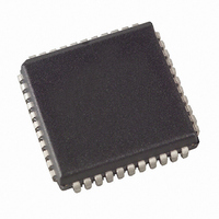
AT89C51RD2-SLSUM Atmel, AT89C51RD2-SLSUM Datasheet - Page 65

AT89C51RD2-SLSUM
Manufacturer Part Number
AT89C51RD2-SLSUM
Description
IC 8051 MCU FLASH 64K 44PLCC
Manufacturer
Atmel
Series
89Cr
Datasheet
1.ATWEBDVK-02RC.pdf
(137 pages)
Specifications of AT89C51RD2-SLSUM
Core Processor
8051
Core Size
8-Bit
Speed
60MHz
Connectivity
SPI, UART/USART
Peripherals
POR, PWM, WDT
Number Of I /o
34
Program Memory Size
64KB (64K x 8)
Program Memory Type
FLASH
Ram Size
2K x 8
Voltage - Supply (vcc/vdd)
2.7 V ~ 5.5 V
Oscillator Type
External
Operating Temperature
-40°C ~ 85°C
Package / Case
44-PLCC
Processor Series
AT89x
Core
8051
Data Bus Width
8 bit
Data Ram Size
2 KB
Interface Type
UART, SPI
Maximum Clock Frequency
60 MHz
Number Of Programmable I/os
32
Number Of Timers
3
Operating Supply Voltage
2.7 V to 5.5 V
Maximum Operating Temperature
+ 85 C
Mounting Style
SMD/SMT
3rd Party Development Tools
PK51, CA51, A51, ULINK2
Minimum Operating Temperature
- 40 C
Package
44PLCC
Device Core
80C51
Family Name
89C
Maximum Speed
40 MHz
For Use With
AT89OCD-01 - USB EMULATOR FOR AT8XC51 MCUAT89STK-11 - KIT STARTER FOR AT89C51RX2
Lead Free Status / RoHS Status
Lead free / RoHS Compliant
Eeprom Size
-
Data Converters
-
Lead Free Status / Rohs Status
Details
Available stocks
Company
Part Number
Manufacturer
Quantity
Price
Company:
Part Number:
AT89C51RD2-SLSUM
Manufacturer:
ATMEL
Quantity:
185 248
Company:
Part Number:
AT89C51RD2-SLSUM
Manufacturer:
CMD
Quantity:
1 993
Part Number:
AT89C51RD2-SLSUM
Manufacturer:
MICROCHIP/微芯
Quantity:
20 000
16.3
16.3.1
4235K–8051–05/08
Functional Description
Operating Modes
Figure 16-2
Figure 16-2. SPI Module Block Diagram
The Serial Peripheral Interface can be configured in one of the two modes: Master mode or
Slave mode. The configuration and initialization of the SPI Module is made through one register:
Once the SPI is configured, the data exchange is made using:
During an SPI transmission, data is simultaneously transmitted (shifted out serially) and
received (shifted in serially). A serial clock line (SCK) synchronizes shifting and sampling on the
two serial data lines (MOSI and MISO). A Slave Select line (SS) allows individual selection of a
Slave SPI device; Slave devices that are not selected do not interfere with SPI bus activities.
When the Master device transmits data to the Slave device via the MOSI line, the Slave device
responds by sending data to the Master device via the MISO line. This implies full-duplex trans-
mission with both data out and data in synchronized with the same clock (Figure 16-3).
• The Serial Peripheral Control register (SPCON)
• SPCON
• The Serial Peripheral STAtus register (SPSTA)
• The Serial Peripheral DATa register (SPDAT)
SPI Interrupt Request
shows a detailed structure of the SPI Module.
Clock
Divider
FCLK PERIPH
SPR2
/128
/16
/32
/64
SPEN
/8
/4
Clock
Select
SSDIS
MSTR
SPIF
Receive Data Register
CPOL
7
WCOL
Shift Register
Internal Bus
6
SPI
Control
CPHA
5
4
3
SPR1
-
2
Clock
Logic
SPCON
1
AT89C51RD2/ED2
SPDAT
MODF
0
SPR0
-
M
Pin
Control
Logic
S
-
-
SPSTA
-
8-bit bus
1-bit signal
MOSI
MISO
SCK
SS
65


