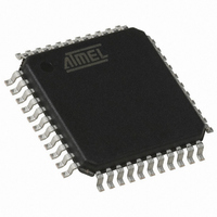
AT89C51CC03CA-RLTUM Atmel, AT89C51CC03CA-RLTUM Datasheet - Page 44

AT89C51CC03CA-RLTUM
Manufacturer Part Number
AT89C51CC03CA-RLTUM
Description
IC 8051 MCU 64K FLASH 44-VQFP
Manufacturer
Atmel
Series
AT89C CANr
Datasheet
1.AT89C51CC03C-S3RIM.pdf
(198 pages)
Specifications of AT89C51CC03CA-RLTUM
Core Processor
8051
Core Size
8-Bit
Speed
40MHz
Connectivity
CAN, UART/USART
Peripherals
POR, PWM, WDT
Number Of I /o
36
Program Memory Size
64KB (64K x 8)
Program Memory Type
FLASH
Eeprom Size
2K x 8
Ram Size
2.25K x 8
Voltage - Supply (vcc/vdd)
3 V ~ 5.5 V
Data Converters
A/D 8x10b
Oscillator Type
External
Operating Temperature
-40°C ~ 85°C
Package / Case
44-TQFP, 44-VQFP
Processor Series
AT89x
Core
8051
Data Bus Width
8 bit
Data Ram Size
2304 B
Interface Type
UART, SPI
Maximum Clock Frequency
60 MHz
Number Of Programmable I/os
36
Number Of Timers
2
Operating Supply Voltage
3 V to 5.5 V
Maximum Operating Temperature
+ 85 C
Mounting Style
SMD/SMT
3rd Party Development Tools
PK51, CA51, A51, ULINK2
Minimum Operating Temperature
- 40 C
On-chip Adc
10 bit, 8 Channel
Package
44VQFP
Device Core
8051
Family Name
AT89
Maximum Speed
60 MHz
For Use With
AT89OCD-01 - USB EMULATOR FOR AT8XC51 MCU
Lead Free Status / RoHS Status
Lead free / RoHS Compliant
Available stocks
Company
Part Number
Manufacturer
Quantity
Price
Company:
Part Number:
AT89C51CC03CA-RLTUM
Manufacturer:
ADI
Quantity:
141
FM0 Memory Architecture
User Space
Extra Row (XRow)
Hardware security Byte (HSB)
Column Latches
Cross Flash Memory Access
Description
44
AT89C51CC03
The Flash memory is made up of 4 blocks (see Figure 23):
•
•
•
•
This space is composed of a 64K Bytes Flash memory organized in 512 pages of 128
Bytes. It contains the user’s application code.
This row is a part of FM0 and has a size of 128 Bytes. The extra row may contain infor-
mation for boot loader usage.
The Hardware security Byte space is a part of FM0 and has a size of 1 byte.
The 4 MSB can be read/written by software (from FM0 and , the 4 LSB can only be read
by software and written by hardware in parallel mode.
H Hardware Security Byte (HSB)
The column latches, also part of FM0, have a size of full page (128 Bytes).
The column latches are the entrance buffers of the three previous memory locations
(user array, XROW and Hardware security byte). The column latches are write only and
can be accessed only from FM1 (boot mode) and from external memory
The FM0 memory can be program only from FM1. Programming FM0 from FM0 or from
external memory is impossible.
The FM1 memory can be program only by parallel programming.
The Table show all software Flash access allowed.
Number
Bit
2-0
The memory array (user space) 64K Bytes
The Extra Row
The Hardware security bits
The column latch registers
X2
7
6
5
4
3
7
Mnemonic
LB2-0
BLJB
BLJB
Bit
X2
-
-
-
6
Description
X2 Mode
Programmed (=’0’) to force X2 mode (6 clocks per instruction) after reset
Unprogrammed to force X1 mode, Standard Mode, afetr reset (Default)
Boot Loader Jump Bit
When unprogrammed (=’1’), at the next reset :
-ENBOOT=0 (see code space memory configuration)
-Start address is 0000h (PC=0000h)
When programmed (=’0’)at the nex reset:
-ENBOOT=1 (see code space memory configuration)
-Start address is F800h (PC=F800h)
Reserved
Reserved
Reserved
General Memory Lock Bits (only programmable by programmer tools)
Section “Flash Protection from Parallel Programming”, page 53
5
-
4
-
3
-
LB2
2
4182O–CAN–09/08
LB1
1
LB0
0


