AT91RM9200-CJ-002 Atmel, AT91RM9200-CJ-002 Datasheet
AT91RM9200-CJ-002
Specifications of AT91RM9200-CJ-002
Available stocks


Related parts for AT91RM9200-CJ-002


AT91RM9200-CJ-002 Summary of contents
Page 1
... Master/Slave Serial Peripheral Interface (SPI) – 16-bit Programmable Data Length, 4 External Peripheral Chip Selects ® ® Thumb Processor ™ (256-ball BGA Package ® ARM920T-based Microcontroller AT91RM9200 NOTE: This is a summary document. The complete document is available on the Atmel website at www.atmel.com. 1768MS–ATARM–09-Jul-09 ...
Page 2
... Flash Card, infrared and Smart Card applications. To complete the offer, the AT91RM9200 benefits from the integration of a wide range of debug features including JTAG-ICE, a dedicated UART debug channel (DBGU) and an embedded real time trace. This enables the development and debug of all applications, especially those with real-time constraints ...
Page 3
... Block Diagram Bold arrows ( Figure 2-1. AT91RM9200 Block Diagram Reset TST0-TST1 and NRST Test JTAGSEL TDI JTAG TDO Scan TMS TCK NTRST FIQ IRQ0-IRQ6 PCK0-PCK3 PLLRCB PLLB PLLRCA PLLA XIN OSC XOUT XIN32 OSC XOUT32 DRXD DTXD PIOA/PIOB/PIOC/PIOD DDM DDP MCCK ...
Page 4
... JTAG Selection TSYNC Trace Synchronization Signal TCLK Trace Clock TPS0 - TPS2 Trace ARM Pipeline Status TPK0 - TPK15 Trace Packet Port NRST Microcontroller Reset TST0 - TST1 Test Mode Select AT91RM9200 4 Active Type Power Power Power Power Power Power Ground Ground Ground Clocks, Oscillators and PLLs ...
Page 5
... Output Input Output EBI for CompactFlash Support Output Output Output Output Output Output Output AT91RM9200 Active Level Comments Debug Receive Data Debug Transmit Data Pulled-up input at reset Pulled-up input at reset Pulled-up input at reset Pulled-up input at reset Pulled-up input at reset 0 at reset ...
Page 6
... Receive Data RTS0 - RTS3 Ready To Send CTS0 - CTS3 Clear To Send DSR1 Data Set Ready DTR1 Data Terminal Ready DCD1 Data Carrier Detect RI1 Ring Indicator AT91RM9200 6 Type EBI for NAND Flash/SmartMedia Support Output Output Output SDRAM Controller Output Output Output Output Output ...
Page 7
... I/O Output Synchronous Serial Controller Output Input I/O I/O I/O I/O Timer/Counter Input I/O I/O AT91RM9200 Active Level Comments RMII only MII only MII only ETX0 - ETX1 only in RMII MII only MII only RMII only ERX0 - ERX1 only in RMII MII only ...
Page 8
... ETM port with outputs multiplexed on the PIO Controller D • a second USB Host transceiver, opening the Hub capabilities of the embedded USB Host. 4.1 208-pin PQFP Package Outline Figure 1-1 A detailed mechanical description is given in the section “AT91RM9200 Mechanical Characteris- tics” of the product datasheet. Figure 4-1. AT91RM9200 8 ...
Page 9
... PQFP Package Pinout Table 4-1. AT91RM9200 Pinout for 208-pin PQFP Package Pin Number Signal Name 1 PC24 2 PC25 3 PC26 4 PC27 5 PC28 6 PC29 7 VDDIOM 8 GND 9 PC30 10 PC31 11 PC10 12 PC11 13 PC12 14 PC13 15 PC14 16 PC15 17 PC0 18 PC1 19 VDDCORE 20 GND 21 PC2 22 PC3 23 PC4 24 PC5 ...
Page 10
... A21 160 A22 Note: 1. Shaded cells define the pins powered by VDDIOM. 4.3 256-ball BGA Package Outline Figure 4-2 A detailed mechanical description is given in the section “AT91RM9200 Mechanical Characteris- tics” of the product datasheet. Figure 4-2. AT91RM9200 10 Pin Pin Number Signal Name ...
Page 11
... BGA Package Pinout Table 4-2. AT91RM9200 Pinout for 256-ball BGA Package Pin Signal Name A1 TDI A2 JTAGSEL A3 PB20 A4 PB17 A5 PD11 A6 PD8 A7 VDDIOP A8 PB9 A9 PB4 A10 PA31/BMS A11 VDDIOP A12 PA23 A13 PA19 A14 GND A15 PA14 A16 VDDIOP A17 PA13 ...
Page 12
... Table 4-2. AT91RM9200 Pinout for 256-ball BGA Package (Continued) Pin Signal Name L1 GND L2 HDPB L3 HDMB GND L6 VDDIOP L12 PC10 L13 PC15 L14 PC2 L15 PC3 L16 VDDCORE L17 PLLRCA M1 VDDIOM M2 GND A1/NBS2/NWR2 M5 A10 GND M9 NCS1/SDCS M11 D4 M12 GND M13 PC13 M14 ...
Page 13
... Ground pins are common to all power supplies, except VDDPLL and VDDOSC pins. For these pins, GNDPLL and GNDOSC are provided, respectively. 5.2 Power Consumption The AT91RM9200 consumes about 500 µA of static current on VDDCORE at 25⋅ C. For dynamic power consumption, the AT91RM9200 consumes a maximum VDDCORE at maximum speed in typical conditions (1.8V, 25⋅ C), processor running full-performance algorithm. ...
Page 14
... Access permission for large pages and small pages can be specified separately for – 16 embedded domains – 64 Entry Instruction TLB and 64 Entry Data TLB 8-, 16-, 32-bit Data Bus for Instructions and Data 7.2 Debug and Test • Integrated EmbeddedICE AT91RM9200 14 ™ -based on ARM Architecture v4T each quarter of the pages 1768MS–ATARM–09-Jul-09 ...
Page 15
... Memory Controller • Programmable Bus Arbiter handling four Masters – Internal Bus is shared by ARM920T, PDC, USB Host Port and Ethernet MAC – Each Master can be assigned a priority between 0 and 7 1768MS–ATARM–09-Jul-09 ™ Rev2a ® connected on SPI NPCS0 Masters AT91RM9200 15 ...
Page 16
... Source, Type and all parameters of the access leading to an abort are saved • Misalignment Detector – Alignment checking of all data accesses – Abort generation in case of misalignment • Remap command – Provides remapping of an internal SRAM in place of the boot NVM AT91RM9200 16 1768MS–ATARM–09-Jul-09 ...
Page 17
... Memories Figure 8-1. AT91RM9200 Memory Mapping Address Memory Space 0x0000 0000 Internal Memories 256M Bytes 0x0FFF FFFF 0x1000 0000 EBI 256M Bytes Chip Select 0 / BFC 0x1FFF FFFF 0x2000 0000 EBI 256M Bytes Chip Select 1 / SDRAMC 0x2FFF FFFF 0x3000 0000 EBI 256M Bytes ...
Page 18
... Remap, the SRAM is also available at address 0x0. 8.1.1.2 Internal ROM The AT91RM9200 integrates a 128-Kbyte Internal ROM. At any time, the ROM is mapped at address 0x10 0000 also accessible at address 0x0 after reset and before the Remap Com- mand if the BMS is tied high during reset. ...
Page 19
... Embeds and controls: – One Main Oscillator and One Slow Clock Oscillator (32.768Hz) – Two Phase Locked Loops (PLLs) and Dividers – Clock Prescalers • Provides: – the Processor Clock PCK 1768MS–ATARM–09-Jul-09 Figure 8-1 on page interrupts External Sources AT91RM9200 17. 19 ...
Page 20
... Input change interrupt – Glitch filter – Multi-drive option enables driving in open drain – Programmable pull up on each I/O line – Pin data status register, supplies visibility of the level on the pin at any time AT91RM9200 20 USB Device Port Generator peripherals 1768MS–ATARM–09-Jul-09 ...
Page 21
... A complete memory map is presented in 10.2 Peripheral Identifiers The AT91RM9200 embeds a wide range of peripherals. tifiers of the AT91RM9200. A peripheral identifier is required for the control of the peripheral interrupt with the Advanced Interrupt Controller and for the control of the peripheral clock with the Power Management Controller. Table 10-1. ...
Page 22
... Peripheral Multiplexing on PIO Lines The AT91RM9200 features four PIO controllers: • PIOA and PIOB, multiplexing I/O lines of the peripheral set • PIOC, multiplexing the data bus bits and several External Bus Interface control signals. Using PIOC pins increases the number of general-purpose I/O lines available but prevents 32-bit memory access • ...
Page 23
... TCLK1 I/O TCLK2 I/O IRQ6 I/O TIOA0 I/O TIOB0 I/O TIOA1 I/O TIOB1 I/O TIOA2 I/O TIOB2 I/O IRQ3 I/O PCK1 I/O IRQ2 I/O IRQ1 I/O TCLK3 I/O TCLK4 I/O TCLK5 I/O CTS2 I/O RTS2 I/O AT91RM9200 Application Usage Function Comments 23 ...
Page 24
... DTR1 PB20 TXD1 PB21 RXD1 PB22 SCK1 PB23 DCD1 PB24 CTS1 PB25 DSR1 PB26 RTS1 PB27 PCK0 PB28 FIQ PB29 IRQ0 AT91RM9200 24 Reset Peripheral B State RTS3 I/O CTS3 I/O SCK3 I/O MCDA1 I/O MCDA2 I/O MCDA3 I/O TIOA3 I/O TIOB3 I/O ...
Page 25
... Reset Peripheral B State I/O I/O I/O I/O I/O I/O I/O A23 A24 A25 NCS4 NCS5 NCS6 NCS7 I/O I/O I/O I/O I/O I/O I/O I/O I/O I/O I/O I/O I/O I/O I/O I/O I/O I/O AT91RM9200 Application Usage Function Comments 25 ...
Page 26
... The PIO Controller D multiplexes pure output signals on peripheral A connections, in particular from the EMAC MII inter- face and the ETM Port on the peripheral B connections. The PIO Controller D is available only in the 256-ball BGA package option of the AT91RM9200. Table 10-5. Multiplexing on PIO Controller D ...
Page 27
... External memory mapping, 512-Mbyte address space • Chip Select Lines • 16-bit Data Bus • Remap of Boot Memory • Multiple Access Modes supported – Byte Write or Byte Select Lines – Two different Read Protocols for each Memory Bank • Multiple device adaptability 1768MS–ATARM–09-Jul-09 AT91RM9200 27 ...
Page 28
... Adaptability to different device access protocols and bus interfaces – Two Burst Read Protocols: Clock Control Address Advance or Signal Controlled – Multiplexed or separate address and data buses – Continuous Burst and Page Mode Accesses supported AT91RM9200 28 Address Advance 1768MS–ATARM–09-Jul-09 ...
Page 29
... Ping-pong mode (two memory banks) for isochronous and bulk endpoints • Six general-purpose endpoints – Endpoint 0, Endpoint 3: 8 bytes, no ping-pong mode – Endpoint 1, Endpoint 2: 64 bytes, ping-pong mode – Endpoint 4, Endpoint 5: 256 bytes, ping-pong mode 10.13 Ethernet MAC • Compatibility with IEEE Standard 802.3 1768MS–ATARM–09-Jul-09 AT91RM9200 29 ...
Page 30
... Programmable Baud Rate Generator • 9-bit full-duplex synchronous or asynchronous serial communications – stop bits in Asynchronous Mode stop bits in Synchronous Mode – Parity generation and error detection – Framing error detection, overrun error detection AT91RM9200 30 peripherals Sensors and data per chip select ...
Page 31
... The USART describes features allowing management of the Modem Signals DTR, DSR, DCD and RI. For details, see In the AT91RM9200, only the USART1 implements these signals, named DTR1, DSR1, DCD1 and RI1. The USART0, USART2 and USART3 do not implement all the modem signals. Only RTS and CTS (RTS0 and CTS0, RTS2 and CTS2, RTS3 and CTS3, respectively) are implemented in these USARTs for other features ...
Page 32
... Two global registers that act on all three TC Channels • The Timer Counter are described with five generic clock inputs, TIMER_CLOCK1 to TIMER_CLOCK5. In the AT91RM9200, these clock inputs are connected to the Master Clock (MCK), to the Slow Clock (SLCK) and to divisions of the Master Clock. For details, see Control” ...
Page 33
... C1 Max Symbol 0.23 b1 0.19 ddd 1.03 1.60 REF aaa 0.3 ccc D D1 0.50 E 3.60 E1 0.27 e AT91RM9200 Min Nom Max 0.17 0.20 0.23 0.10 Tolerances of Form and Position 0.25 0.1 BSC 31.20 28.00 31.20 28.00 0.50 33 ...
Page 34
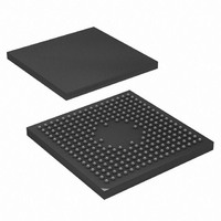
... Figure 11-2. 256-ball BGA Package Drawing AT91RM9200 34 1768MS–ATARM–09-Jul-09 ...
Page 35
... AT91RM9200 Ordering Information Table 12-1. Ordering Information Ordering Code AT91RM9200-QU-002 AT91RM9200-CJ-002 1768MS–ATARM–09-Jul-09 Package Package Type PQFP 208 Green BGA 256 RoHS-compliant AT91RM9200 Temperature Operating Range Industrial (-40⋅ 85⋅ ...
Page 36
... CSR 03-209 • Page 3; Figure 1: NWAIT pin added to block diagram. CSR 03-244 • Page 14; Table 1. AT91RM9200 Pinout for 208-lead PQFP package, pins 28, 30, 37 and 39 names changed CSR 04-315 • Page 23; Table 7. Pin Description, ICE and JTAG description, “Internal Pullup” added to comments for all signals, except TDO ...
Page 37
... Section 11. “Package Drawings” on page Updated “Features” details on package options. 1768KS Updated Table 40-1, “Ordering Information,” on page Ordering code AT91RM9200-CI-002 removed from 1768LS Ordering Information” on page 35 1768MS USART3 0XFFECC000 changed into 0XFFFCC000 in 1768MS–ATARM–09-Jul-09 Section 8. ”Memories” on page 17 ...
Page 38
... AT91RM9200 38 1768MS–ATARM–09-Jul-09 ...
Page 39
... AT91RM9200 39 ...
Page 40
... AT91RM9200 40 1768MS–ATARM–09-Jul-09 ...
Page 41
... Disclaimer: The information in this document is provided in connection with Atmel products. No license, express or implied, by estoppel or otherwise, to any intellectual property right is granted by this document or in connection with the sale of Atmel products. EXCEPT AS SET FORTH IN ATMEL’S TERMS AND CONDI- TIONS OF SALE LOCATED ON ATMEL’S WEB SITE, ATMEL ASSUMES NO LIABILITY WHATSOEVER AND DISCLAIMS ANY EXPRESS, IMPLIED OR STATUTORY WARRANTY RELATING TO ITS PRODUCTS INCLUDING, BUT NOT LIMITED TO, THE IMPLIED WARRANTY OF MERCHANTABILITY, FITNESS FOR A PARTICULAR PURPOSE, OR NON-INFRINGEMENT ...