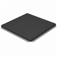
LPC2420FBD208,551 NXP Semiconductors, LPC2420FBD208,551 Datasheet - Page 36

LPC2420FBD208,551
Manufacturer Part Number
LPC2420FBD208,551
Description
IC ARM7 MCU ROMLESS 208LQFP
Manufacturer
NXP Semiconductors
Series
LPC2400r
Datasheet
1.LPC2460FBD208551.pdf
(79 pages)
Specifications of LPC2420FBD208,551
Program Memory Type
ROMless
Package / Case
208-LQFP
Core Processor
ARM7
Core Size
16/32-Bit
Speed
72MHz
Connectivity
EBI/EMI, I²C, Microwire, MMC, SPI, SSI, SSP, UART/USART, USB OTG
Peripherals
Brown-out Detect/Reset, DMA, I²S, POR, PWM, WDT
Number Of I /o
160
Ram Size
82K x 8
Voltage - Supply (vcc/vdd)
3 V ~ 3.6 V
Data Converters
A/D 8x10b; D/A 1x10b
Oscillator Type
Internal
Operating Temperature
-40°C ~ 85°C
Processor Series
LPC24
Core
ARM7TDMI-S
Data Bus Width
16 bit, 32 bit
Data Ram Size
82 KB
Interface Type
CAN/I2C/I2S/SPI/SSP/UART/USB
Maximum Clock Frequency
72 MHz
Number Of Programmable I/os
160
Number Of Timers
4
Operating Supply Voltage
3.3 V
Maximum Operating Temperature
+ 85 C
Mounting Style
SMD/SMT
3rd Party Development Tools
MDK-ARM, RL-ARM, ULINK2
Minimum Operating Temperature
- 40 C
On-chip Adc
8-ch x 10-bit
On-chip Dac
1-ch x 10-bit
Lead Free Status / RoHS Status
Lead free / RoHS Compliant
Eeprom Size
-
Program Memory Size
-
Lead Free Status / Rohs Status
Lead free / RoHS Compliant
Other names
568-4527
935286745551
935286745551
Available stocks
Company
Part Number
Manufacturer
Quantity
Price
Company:
Part Number:
LPC2420FBD208,551
Manufacturer:
NXP Semiconductors
Quantity:
10 000
NXP Semiconductors
LPC2420_60_5
Preliminary data sheet
7.17.1 Features
7.18.1 Features
7.18 I
7.19 I
The LPC2420/2460 contains three I
The I
(SCL), and a serial data line (SDA). Each device is recognized by a unique address and
can operate as either a receiver-only device (e.g., an LCD driver) or a transmitter with the
capability to both receive and send information (such as memory). Transmitters and/or
receivers can operate in either master or slave mode, depending on whether the chip has
to initiate a data transfer or is only addressed. The I
be controlled by more than one bus master connected to it.
The I
I
The I
2
2
2
•
•
•
•
•
C-bus).
•
•
•
•
•
•
•
•
•
•
C-bus serial I/O controller
S-bus serial I/O controllers
The MCI provides all functions specific to the SD/MMC memory card. These include
the clock generation unit, power management control, and command and data
transfer.
Conforms to Multimedia Card Specification v2.11.
Conforms to Secure Digital Memory Card Physical Layer Specification, v0.96.
Can be used as a multimedia card bus or a secure digital memory card bus host. The
SD/MMC can be connected to several multimedia cards or a single secure digital
memory card.
DMA supported through the GPDMA controller.
I
I
devices connected to the same bus lines.
Easy to configure as master, slave, or master/slave.
Programmable clocks allow versatile rate control.
Bidirectional data transfer between masters and slaves.
Multi-master bus (no central master).
Arbitration between simultaneously transmitting masters without corruption of serial
data on the bus.
Serial clock synchronization allows devices with different bit rates to communicate via
one serial bus.
Serial clock synchronization can be used as a handshake mechanism to suspend and
resume serial transfer.
The I
2
2
2
2
2
C0 is a standard I
C1 and I
C-bus is bidirectional, for inter-IC control using only two wires: a serial clock line
C-bus implemented in LPC2420/2460 supports bit rates up to 400 kbit/s (Fast
S-bus provides a standard communication interface for digital audio applications.
2
C-bus can be used for test and diagnostic purposes.
2
C2 use standard I/O pins and do not support powering off of individual
Rev. 05 — 24 February 2010
2
C compliant bus interface with open-drain pins.
2
C-bus controllers.
Flashless 16-bit/32-bit microcontroller
2
C-bus is a multi-master bus and can
LPC2420/2460
© NXP B.V. 2010. All rights reserved.
36 of 79


