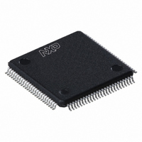
LPC1768FBD100,551 NXP Semiconductors, LPC1768FBD100,551 Datasheet - Page 16

LPC1768FBD100,551
Manufacturer Part Number
LPC1768FBD100,551
Description
IC ARM CORTEX MCU 512K 100-LQFP
Manufacturer
NXP Semiconductors
Series
LPC17xxr
Datasheets
1.OM11043.pdf
(79 pages)
2.LPC1765FBD100551.pdf
(74 pages)
3.LPC1769FBD100551.pdf
(66 pages)
Specifications of LPC1768FBD100,551
Program Memory Type
FLASH
Program Memory Size
512KB (512K x 8)
Package / Case
100-LQFP
Core Processor
ARM® Cortex-M3™
Core Size
32-Bit
Speed
100MHz
Connectivity
CAN, Ethernet, I²C, IrDA, Microwire, SPI, SSI, UART/USART, USB OTG
Peripherals
Brown-out Detect/Reset, DMA, I²S, Motor Control PWM, POR, PWM, WDT
Number Of I /o
70
Ram Size
64K x 8
Voltage - Supply (vcc/vdd)
2.4 V ~ 3.6 V
Data Converters
A/D 8x12b, D/A 1x10b
Oscillator Type
Internal
Operating Temperature
-40°C ~ 85°C
Processor Series
LPC17
Core
ARM Cortex M3
Data Bus Width
32 bit
Data Ram Size
64 KB
Interface Type
CAN, I2C, SPI, UART
Maximum Clock Frequency
100 MHz
Number Of Programmable I/os
70
Number Of Timers
3
Operating Supply Voltage
3.3 V
Maximum Operating Temperature
+ 85 C
Mounting Style
SMD/SMT
3rd Party Development Tools
MDK-ARM, RL-ARM, ULINK2, MCB1760, MCB1760U, MCB1760UME, IRD-LPC1768-DEV, KSK-LPC1768-JL
Development Tools By Supplier
OM11032, OM11033, OM11034, OM11035, OM11043
Minimum Operating Temperature
- 40 C
On-chip Adc
12 bit, 8 Channel
On-chip Dac
10 bit
Package
100LQFP
Device Core
ARM Cortex M3
Family Name
LPC17xx
Maximum Speed
100 MHz
Cpu Family
LPC17xx
Device Core Size
32b
Frequency (max)
100MHz
Total Internal Ram Size
64KB
# I/os (max)
70
Number Of Timers - General Purpose
4
Operating Supply Voltage (typ)
3.3V
Operating Supply Voltage (max)
3.6V
Operating Supply Voltage (min)
2.4V
Instruction Set Architecture
RISC
Operating Temp Range
-40C to 85C
Operating Temperature Classification
Industrial
Mounting
Surface Mount
Pin Count
100
Package Type
LQFP
Lead Free Status / RoHS Status
Lead free / RoHS Compliant
For Use With
568-4916 - DEVELOPMENT BOARD LPC1768 MBED568-4816 - EVAL BOARD FOR MCB1768568-4815 - KIT EVAL LPC1768 CR622-1032 - KIT DEV IND REF DESIGN LPC1768622-1005 - USB IN-CIRCUIT PROG ARM7 LPC2K
Eeprom Size
-
Lead Free Status / Rohs Status
Lead free / RoHS Compliant
Other names
568-4796
935288608551
935288608551
Available stocks
Company
Part Number
Manufacturer
Quantity
Price
Company:
Part Number:
LPC1768FBD100,551
Manufacturer:
NXP Semiconductors
Quantity:
10 000
Part Number:
LPC1768FBD100,551
Manufacturer:
NXP/恩智浦
Quantity:
20 000
NXP Semiconductors
Table 4.
[1]
[2]
[3]
LPC1769_68_67_66_65_64_63
Product data sheet
Symbol
TDI
TMS/SWDIO
TRST
TCK/SWDCLK
RTCK
RSTOUT
RESET
XTAL1
XTAL2
RTCX1
RTCX2
V
V
V
V
V
VREFP
VREFN
VBAT
n.c.
SS
SSA
DD(3V3)
DD(REG)(3V3)
DDA
5 V tolerant pad providing digital I/O functions with TTL levels and hysteresis.
5 V tolerant pad providing digital I/O functions (with TTL levels and hysteresis) and analog input. When configured as a ADC input,
digital section of the pad is disabled and the pin is not 5 V tolerant.
5 V tolerant pad providing digital I/O with TTL levels and hysteresis and analog output function. When configured as the DAC output,
digital section of the pad is disabled.
Pin description
Pin
2
3
4
5
100
14
17
22
23
16
18
31, 41,
55, 72,
83, 97
11
28, 54,
71, 96
42, 84
10
12
15
19
13
[1][8]
[1][8]
[1][8]
[1][7]
[10]
[9]
[10][11]
[10][11]
[10][12]
[10]
[10]
[10]
[10][12]
[1][7]
[10]
[10]
[10]
…continued
Ball
C3
B1
C2
C1
B2
-
F3
H2
G3
F2
G1
B3, B7,
C9, G7,
J6, K3
E1
K2, H9,
C10,
A3
H6, A7
E2
E3
F1
G2
D4, E4
[1][8]
[1][7]
[9]
[10][11]
[10]
[10]
[10]
[10]
[1][8]
[1][8]
[1][7]
[10][11]
[10][11]
[10]
[10][12]
[10]
[10]
All information provided in this document is subject to legal disclaimers.
Type
I
I
I/O
I
I
I
O
O
I
I
O
I
O
I
I
I
I
I
I
I
I
-
Rev. 6.01 — 11 March 2011
Description
TDI — Test Data in for JTAG interface.
TMS — Test Mode Select for JTAG interface.
SWDIO — Serial wire debug data input/output.
TRST — Test Reset for JTAG interface.
TCK — Test Clock for JTAG interface.
SWDCLK — Serial wire clock.
RTCK — JTAG interface control signal.
RSTOUT — This is a 3.3 V pin. LOW on this pin indicates the
microcontroller being in Reset state.
External reset input: A LOW on this pin resets the device, causing I/O
ports and peripherals to take on their default states, and processor
execution to begin at address 0. TTL with hysteresis, 5 V tolerant.
Input to the oscillator circuit and internal clock generator circuits.
Output from the oscillator amplifier.
Input to the RTC oscillator circuit.
Output from the RTC oscillator circuit.
ground: 0 V reference.
analog ground: 0 V reference. This should nominally be the same
voltage as V
3.3 V supply voltage: This is the power supply voltage for the I/O
ports.
3.3 V voltage regulator supply voltage: This is the supply voltage for
the on-chip voltage regulator only.
analog 3.3 V pad supply voltage: This should be nominally the same
voltage as V
This voltage is used to power the ADC and DAC. This pin should be
tied to 3.3 V if the ADC and DAC are not used.
ADC positive reference voltage: This should be nominally the same
voltage as V
Level on this pin is used as a reference for ADC and DAC. This pin
should be tied to 3.3 V if the ADC and DAC are not used.
ADC negative reference voltage: This should be nominally the same
voltage as V
Level on this pin is used as a reference for ADC and DAC.
RTC pin power supply: 3.3 V on this pin supplies the power to the
RTC peripheral.
not connected.
LPC1769/68/67/66/65/64/63
SS
DD(3V3)
DDA
SS
, but should be isolated to minimize noise and error.
but should be isolated to minimize noise and error.
but should be isolated to minimize noise and error.
but should be isolated to minimize noise and error.
32-bit ARM Cortex-M3 microcontroller
© NXP B.V. 2011. All rights reserved.
16 of 79


