W78C032C40PL Nuvoton Technology Corporation of America, W78C032C40PL Datasheet
W78C032C40PL
Specifications of W78C032C40PL
Available stocks


Related parts for W78C032C40PL

W78C032C40PL Summary of contents
Page 1
Table of Contents- 1. GENERAL DESCRIPTION ......................................................................................................... 2 2. FEATURES ................................................................................................................................. 2 3. PIN CONFIGURATIONS ............................................................................................................ 3 4. PIN DESCRIPTION..................................................................................................................... 4 5. FUNCTIONAL DESCRIPTION ................................................................................................... 6 5.1 TIMERS 0, 1, AND 2....................................................................................................... 6 5.2 CLOCK............................................................................................................................ 6 5.2.1 CRYSTAL OSCILLATOR .................................................................................................6 ...
Page 2
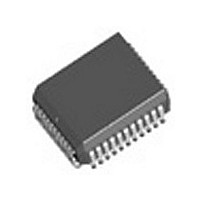
... Four 8-bit bidirectional port Three 16-bit timer/coun ters One full duplex serial port Boolean processor Six-source, two-level interrupt capability Built-in power management Packages: − Lead Free (RoHS) DIP 40: − Lead Free (RoHS) PLCC 44: W78C032C40PL − Lead Free (RoHS) PQFP 44: W78C032C40FL ce ress space s W78C032C40DL - 2 - W78C32C/W78C032C ...
Page 3
PIN CONFIGURATIONS 40-Pin DIP 44-Pin PLCC ...
Page 4
PIN DESCRIPTION P0.0−P0.7 Port 0, Bits 0 through 7. Port bidirectional I/O port. This port also provides a multiplexed low order address/data bus during accesses to external memory. P1.0−P1.7 Port 1, Bits 0 through 7. Port ...
Page 5
PSEN Program Store Enable Output, active low. address/data bus during fetch and MOVC operations. weak pull-up. XTAL1 Crystal 1. This is the crystal oscillator input. This pin may be driven by an external clock. XTAL2 Crystal 2. This is the ...
Page 6
FUNCTIONAL DESCRIPTION The W78C032C architecture consists of a core controller surrounded by various registers, four general purpose I/O ports, 256 bytes of RAM, three timer/counters, and a serial port. The processor supports 111 different instruction and references both a ...
Page 7
Power-down Mode When the PD bit of the PCON register is set, the processor enters the power-down mode. In this mode all of the clocks, including the oscillator are stopped. The only way to exit power-down mode is by ...
Page 8
ELECTRICAL CHARACTERISTICS 6.1 Absolute Maximum Ratings PARAMETER DC Power Supply Input Voltage Operating Temperature Storage Temperature Note: Exposure to conditions beyond those listed under Absolute Maximum Ratings may adversely affect the life and reliability of the device. 6.2 D.C. ...
Page 9
DC Characteristics, continued PARAMETER SYM. Input Low Voltage V IL2 (*3) XTAL1, RST Input High Voltage V IH1 P1, P3 Input High Voltage V IH2 (*3) XTAL1, RST Notes and P2 are in external access mode. 2. RST ...
Page 10
Program Fetch Cycle PARAMETER Address Valid to ALE Low Address Hold after ALE Low ALE Low to PSEN Low PSEN Low to Data Valid Data Hold after PSEN High Data Float after PSEN High ALE Pulse Width PSEN Pulse ...
Page 11
Data Write Cycle PARAMETER ALE Low to WR Low Data Valid to WR Low Data Hold from WR High WR Pulse Width Note: " Δ " ( due to buffer driving delay and wire loading nS. 6.3.5 ...
Page 12
TIMING WAVEFORMS 7.1 Program Fetch Cycle S1 S2 XTAL1 ALE PSEN PORT 2 T AAH PORT 0 A0-A7 Code 7.2 Data Read Cycle S4 S5 XTAL1 ALE PSEN PORT 2 A0-A7 PORT ...
Page 13
Timing Waveforms, continued 7.3 Data Write Cycle S4 S5 XTAL1 ALE PSEN PORT 2 PORT 0 A0- DAW 7.4 Port Access Cycle XTAL1 ALE T PDS PORT INPUT SAMPLE W78C32C/W78C032C A8-A15 DATA OUT ...
Page 14
TYPICAL APPLICATION CIRCUIT 8.1 Using External Program Memory and Crystal XTAL1 XTAL2 CRYSTAL 8 RST C1 C2 INT0 12 13 INT1 P1.0 2 ...
Page 15
Expanded External Data Memory and Oscillator XTAL1 OSCILLATOR XTAL2 8 RST INT0 12 13 INT1 P1.0 2 P1.1 3 P1.2 4 P1.3 5 P1.4 ...
Page 16
PACKAGE DIMENSIONS 9.1 40-pin DIP 9.2 44-pin PLCC θ ...
Page 17
Package Dimensions, continued 9.3 44-pin QFP See Detail F y Seating Plane W78C32C/W78C032C θ Detail F 1 ...
Page 18
REVISION HISTORY VERSION DATE A2 July 1999 A3 June, 2004 A4 April 19, 2005 A5 June 7, 2005 A6 December 4, 2006 Winbond products are not designed, intended, authorized or warranted for use as components in systems or equipment ...