Z8F0422SJ020EG Zilog, Z8F0422SJ020EG Datasheet
Z8F0422SJ020EG
Specifications of Z8F0422SJ020EG
Z8F0422SJ020EG


Related parts for Z8F0422SJ020EG


Z8F0422SJ020EG Summary of contents
Page 1
... High Performance 8-Bit Microcontrollers Z8 Encore! XP Series Product Specification Product Specification PS022517-0508 ® Copyright ©2008 by Zilog , Inc. All rights reserved. www.zilog.com ® F0822 ...
Page 2
... TECHNOLOGY DESCRIBED HEREIN OR OTHERWISE. The information contained within this document has been verified according to the general principles of electrical and mechanical engineering. Z8, Z8 Encore!, Z8 Encore! XP, Z8 Encore! MC, Crimzon, eZ80, and ZNEO are trademarks or registered trademarks of Zilog, Inc. All other product or service names are the property of their respective owners. PS022517-0508 ® ...
Page 3
... Removed Flash Microcontrollers from the title throughout the document. Updated the flag status for BCLR, BIT, and BSET in Table 126. Updated Zilog logo, Zilog text, Disclaimer section, and implemented style guide. Updated Z8 Encore! 8K Series to Z8 Encore! XP F0822 Series Flash Microcontrollers throughout the document. ...
Page 4
Table of Contents Introduction . . . . . . . . . . . . . . . . . . . . . . . . . . . . . . . . . . . . ...
Page 5
Reset Sources . . . . . . . . . . . . . . . . . . . . . . . . . . . . . . . . . . . . . . ...
Page 6
Operation . . . . . . . . . . . . . . . . . . . . . . . . . . . . . . . . . . . . . . . ...
Page 7
Operation . . . . . . . . . . . . . . . . . . . . . . . . . . . . . . . . . . . . . . . ...
Page 8
I2C Diagnostic Control Register . . . . . . . . . . . . . . . . . . . . . . . . . . . . . . . . . 145 Analog-to-Digital Converter ...
Page 9
OCD Interface . . . . . . . . . . . . . . . . . . . . . . . . . . . . . . . . . . . . . . ...
Page 10
... We have designed this Product Specification to be used either as a how to procedural manual or a reference guide to important data. Intended Audience This document is written for Zilog customers who are experienced at working with micro- controllers, integrated circuits, or printed circuit assemblies. Manual Conventions ...
Page 11
Braces The curly braces { }, indicate a single register or bus created by concatenating some com- bination of smaller registers, buses, or individual bits. • Example: The 12-bit register address { hexadecimal value ( (RP) and Working Register R1. ...
Page 12
Use of All Uppercase Letters The use of all uppercase letters designates the names of states, modes, and commands. • Example 1: The bus is considered BUSY after the Start condition. • Example 2: A START command triggers the processing ...
Page 13
Abbreviations/ Acronyms PDIP SOIC SSOP PC IRQ PS022517-0508 Expansion Plastic Dual Inline Package Small Outline Integrated Circuit Small Shrink Outline Package Program Counter Interrupt Request ® Z8 Encore! XP F0822 Series Product Specification Introduction xiii ...
Page 14
... Introduction Zilog’s Z8 Encore! XP the 8-bit eZ8 CPU. Z8 Encore! XP the 8K Series adds Flash memory to Zilog’s extensive line of 8-bit microcontrollers. The Flash in-circuit programming allows faster development time and program changes in the field. The new eZ8 CPU is upward-compatible with the existing Z8 ...
Page 15
V to 3.6 V operating voltage with 5 V-tolerant inputs • 20-pin and 28-pin packages • 0 °C to +70 °C standard temperature and -40 °C to +105 °C extended temperature operating ranges Part Selection Guide Table 1 ...
Page 16
... UART IrDA GPIO Figure 1. Z8 Encore! XP CPU and Peripheral Overview eZ8 CPU Features Zilog’s latest eZ8 8-bit CPU, meets the continuing demand for faster and more code-effi- cient microcontrollers. The eZ8 CPU executes a superset of the original Z8 set. PS022517-0508 On-Chip Debugger ...
Page 17
... C-Compiler friendly. • clock cycles per instruction. For more information regarding the eZ8 CPU, refer to eZ8 CPU Core User Manual (UM0128) available for download at www.zilog.com. General Purpose Input/Output ® Z8 Encore! XP Input/Output (GPIO). The number of GPIO pins available is a function of package. Each pin is individually programmable ...
Page 18
I C The Inter-Integrated Circuit ( protocol. The I (SDA) line, and a serial clock (SCL) line. Serial Peripheral Interface The Serial Peripheral Interface (SPI) allows the Z8 Encore exchange data between other peripheral ...
Page 19
PS022517-0508 ® Z8 Encore! XP F0822 Series Product Specification Introduction 6 ...
Page 20
Signal and Pin Descriptions ® Z8 Encore! XP pin configurations. This chapter describes the signals and available pin configurations for each of the package styles. For information regarding the physical package specifications, see Packaging on page 233. Available Packages Table ...
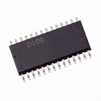
Page 21
PA6 / SCL PA7 / SDA PA0 / T0IN PA1 / T0OUT PA2 / DE0 Figure 2. Z8F0821 and Z8F0421 in 20-Pin SSOP and PDIP Packages PA1 / T0OUT Figure 3. Z8F0822 and Z8F0422 in 28-Pin SOIC and PDIP Packages ...
Page 22
PC0 / T1IN PA6 / SCL PA7 / SDA PC5 / MISO PC4 / MOSI PC3 / SCK PC2 / SS PA0 / T0IN PA1 / T0OUT Figure 5. Z8F0812 and Z8F0412 in 28-Pin SOIC and PDIP Packages Signal Descriptions ...
Page 23
Table 3. Signal Descriptions (Continued) Signal Mnemonic I/O Description SPI Controller SS I/O Slave Select—This signal can be an output or an input. If the is the SPI Master, this pin can be configured as the Slave Select output. If ...
Page 24
Table 3. Signal Descriptions (Continued) Signal Mnemonic I/O Description Oscillators XIN I External Crystal Input—This is the input pin to the crystal oscillator. A crystal is connected between the external crystal input and the oscillator. In addition, this pin is ...
Page 25
Pin Characteristics Table 4 provides detailed information on the characteristics for each pin available on ® Z8 Encore! XP symbol mnemonic. Table 4. Pin Characteristics Symbol Reset Mnemonic Direction Direction AV N/A N N/A N/A SS DBG I/O ...
Page 26
... These three address spaces are covered briefly in the following sections. For more infor- mation on the eZ8 CPU and its address space, refer to eZ8 CPU Core User Manual (UM0128) available for download at www.zilog.com. Register File The Register File address space in the Z8 Encore! XP posed of two sections— ...
Page 27
Table 5. Z8 Encore! XP F0822 Series Program Memory Maps Program Memory Address (Hex) Z8F082x and Z8F081x Products 0000-0001 0002-0003 0004-0005 0006-0007 0008-0037 0038-1FFF Z8F042x and Z8F041x Products 0000-0001 0002-0003 0004-0005 0006-0007 0008-0037 0038-0FFF Note: *See Table 24 on ...
Page 28
Register File Address Map Table 7 provides the address map for the Register File of the Z8 Encore! XP Series products. Not all devices and package styles in the F0822 Series support the ADC, the SPI, or all of the ...
Page 29
Table 7. Register File Address Map (Continued) Address (Hex) Register Description F47 UART0 Baud Rate Low Byte F48-F4F Reserved F50 I C Data 2 F51 I C Status 2 F52 I C Control 2 F53 I ...
Page 30
Table 7. Register File Address Map (Continued) Address (Hex) Register Description FCE Reserved FCF Interrupt Control GPIO Port A FD0 Port A Address FD1 Port A Control FD2 Port A Input Data FD3 Port A Output Data GPIO Port B ...
Page 31
Table 7. Register File Address Map (Continued) Address (Hex) Register Description FFC Flags FFD Register Pointer FFE Stack Pointer High Byte FFF Stack Pointer Low Byte XX=Undefined PS022517-0508 ® Z8 Encore! XP F0822 Series Product Specification Mnemonic Reset (Hex) Page ...
Page 32
Control Register Sum- mary Timer 0 High Byte T0H (F00H - Read/Write Timer 0 current count value Timer 0 Low Byte T0L (F01H - Read/Write ...
Page 33
Timer 1 Reload Low Byte T1RL (F0BH - Read/Write Timer 1 reload value [7:0] Timer 1 PWM High Byte T1PWMH (F0CH - Read/Write Timer ...
Page 34
UART0 Status 0 U0STAT0 (F41H - Read Only CTS signal Returns the level of the CTS signal Transmitter Empty 0 = Data is currently transmitting 1 = Transmission is complete Transmitter Data ...
Page 35
PS022517-0508 Z8 Encore! XP Product Specification UART0 Control 1 U0CTL1 (F43H - Read/Write Infrared Encoder/Decoder 0 = Infrared endec is disabled 1 = Infrared endec is enabled Received Data Interrupt 0 = ...
Page 36
UART0 Status 1 U0STAT1 (F44H- Read Only Mulitprocessor Receive Returns value of last multiprocessor bit New Frame 0 = Current byte is not start of frame 1 = Current byte is start ...
Page 37
PS022517-0508 Z8 Encore! XP Product Specification I2C Control I2CCTL (F52H - Read/Write I2C Signal Filter Enable 0 = Digital filtering disabled 1 = Low-pass digital filters enabled on SDA and SCL input ...
Page 38
I2C Baud Rate Generator High Byte I2CBRH (F53H - Read/Write I2C Baud Rate divisor [15:8] I2C Baud Rate Generator Low Byte I2CBRL (F54H - Read/Write ...
Page 39
SPI Status SPISTAT (F62H - Read Only Slave Select Slave, SS pin is asserted Slave, SS pin is not asserted Transmit Status data ...
Page 40
SPI Diagnostic State SPIDST (F64H - Read Only SPI State Transmit Clock Enable 0 = Internal transmit clock enable signal is deasserted 1 = Internal transmit clock enable signal is asserted Shift ...
Page 41
ADC Control ADCCTL (F70H - Read/Write Analog Input Select 0000 = ANA0 ANA1 0010 = ANA2 ANA3 0100 = ANA4 0101 through 21111 = Reserved Continuous Mode Select 0 = Single-shot conversion ...
Page 42
Interrupt Request 0 IRQ0 (FC0H - Read/Write ADC Interrupt Request SPI Interrupt Request I2C Interrupt Request UART 0 Transmitter Interrupt UART 0 Receiver Interrupt Timer 0 Interrupt Request Timer 1 Interrupt Request ...
Page 43
IRQ0 Enable Low Bit IRQ0ENL (FC2H - Read/Write ADC IRQ Enable Hit Bit SPI IRQ Enable Low Bit I2C IRQ Enable Low Bit UART 0 Transmitter IRQ UART 0 Receiver IRQ Enable ...
Page 44
Interrupt Request 2 IRQ2 (FC6H - Read/Write Port C Pin Interrupt Request 0 = IRQ from corresponding pin [3:0] is not pending 1 = IRQ from corresponding pin [3:0] is awaiting service ...
Page 45
Port A Address PAADDR (FD0H - Read/Write Port A Address[7:0] Selects Port Sub-Registers: 00H = No function 01H = Data direction 02H = Alternate function 03H = Output control (open- drain) 04H ...
Page 46
Port B Address PBADDR (FD4H - Read/Write Port B Address[7:0] Selects Port Sub-Registers: 00H = No function 01H = Data direction 02H = Alternate function 03H = Output control (open- drain) 04H ...
Page 47
Port C Address PCADDR (FD8H - Read/Write Port C Address[7:0] Selects Port Sub-Registers: 00H = No function 01H = Data direction 02H = Alternate function 03H = Output control (open- drain) 04H ...
Page 48
Watchdog Timer Control WDTCTL (FF0H - Read Only configuration indicator Reserved EXT 0 = Reset not generated by RESET pin 1 = Reset generated by RESET pin WDT 0 = WDT ...
Page 49
Flash Control FCTL (FF8H - Write Only Flash Command 73H = First unlock command 8CH = Second unlock command 95H = Page erase command 63H = Mass erase command 5EH = Flash ...
Page 50
Flash Sector Protect FPROT (FF9H - Read/Write to 1’ Flash Sector Protect [7: Sector can be programmed or erased from user code 1 = Sector is protected and cannot be ...
Page 51
Register Pointer RP (FFDH- Read/Write Working Register Group Stack Pointer High Byte SPH (FFEH - Read/Write Stack Pointer [15:8] Stack Pointer Low Byte SPL ...
Page 52
Reset and Stop Mode Recovery The Reset Controller within the Z8 Encore! XP Mode Recovery operation. In typical operation, the following events cause a Reset to occur: • Power-On Reset (POR) • Voltage Brownout • WDT time-out (when configured through ...
Page 53
System Reset During a System Reset Encore! XP cycles of the WDT oscillator followed by 16 cycles of the system clock. At the beginning of Reset, all GPIO pins are configured as inputs. All GPIO programmable pull-ups are ...
Page 54
Power-On Reset Each device in the Z8 Encore! XP POR circuit monitors the supply voltage and holds the device in the Reset state until the supply voltage reaches a safe operating level. After the supply voltage exceeds the POR voltage ...
Page 55
POR voltage threshold (V Reset state. After the supply voltage again exceeds the POR voltage threshold, the device progresses through a full System Reset sequence as described in the POR section. Following POR, the POR status bit ...
Page 56
External Pin Reset The RESET pin contains a Schmitt-triggered input, an internal pull-up, an analog filter, and a digital filter to reject noise. After the RESET pin is asserted for at least 4 system clock cycles, the device progresses through ...
Page 57
Stop Mode Recovery Using WDT Time-Out If the WDT times out during STOP mode, the device undergoes a Stop Mode Recovery sequence. In the WDT Control Register, the WDT and STOP bits are set the WDT is ...
Page 58
Low-Power Modes ® Z8 Encore power reduction is provided by STOP mode. The next level of power reduction is pro- vided by the HALT mode. STOP Mode Execution of the eZ8 CPU’s STOP instruction places the device into ...
Page 59
WDT’s internal RC oscillator continues to operate. • If enabled, the WDT continues to operate. • All other on-chip peripherals continue to operate. The eZ8 CPU can be brought out of HALT mode by any of the following operations: ...
Page 60
General-Purpose Input/Output ® Z8 Encore! XP for General-Purpose Input/Output (GPIO) operations. Each port consists Control and Data Registers. The GPIO Control Registers are used to determine data direction, open-drain, output drive current, programmable pull-ups, Stop Mode Recovery functionality, and alternate ...
Page 61
Port Output Data Register DATA D Q Bus System Clock Figure 8. GPIO Port Pin Block Diagram Table 12. Port Alternate Function Mapping Port Pin Port A PA0 PA1 PA2 PA3 PA4 PA5 PA6 PA7 Port B PB0 PB1 PB2 ...
Page 62
Table 12. Port Alternate Function Mapping (Continued) Port Pin Port C PC0 PC1 PC2 PC3 PC4 PC5 GPIO Interrupts Many of GPIO port pins are used as interrupt sources. Some port pins are configured to generate an interrupt request on ...
Page 63
Table 13. GPIO Port Registers and Sub-Registers (Continued) Port Register Mnemonic PxOC PxHDE PxSMRE PxPUE Port A–C Address Registers The Port A–C Address Registers select the GPIO Port functionality accessible through the Port A–C Control Registers. The Port A–C Address ...
Page 64
Port A–C Control Registers The Port A–C Control Registers set the GPIO port operation. The value in the correspond- ing Port A–C Address Register determines the control sub-registers accessible using the Port A–C Control Register Table 15. Port A–C Control ...
Page 65
Block Diagram on page 48. Caution: Do not enable alternate function for GPIO port pins which do not have an associated alternate function. Failure to follow this guideline can ...
Page 66
The drain of the associated pin is disabled (open-drain mode). Port A–C High Drive Enable Sub-Registers The Port A–C High Drive Enable sub-register Port A–C Control Register by writing bits in the Port A–C High Drive ...
Page 67
The port pin is configured as a Stop Mode Recovery source. Any logic transition on this pin during STOP mode initiates Stop Mode Recovery. Port A–C Pull-up Enable Sub-Registers The Port A–C Pull-Up Enable sub-register Control Register by ...
Page 68
Port A–C Output Data Register The Port A–C Output Data Register Table 23. Port A–C Output Data Register (PxOUT) BITS 7 6 POUT7 POUT6 FIELD RESET R/W ADDR POUT[7:0]—Port Output Data These bits contain the data to be driven to ...
Page 69
PS022517-0508 ® Z8 Encore! XP F0822 Series Product Specification General-Purpose Input/Output 56 ...
Page 70
... The eZ8 CPU supports both vectored and polled interrupt handling. For polled interrupts, the interrupt control has no effect on operation. For more information on interrupt servic- ing, refer to eZ8 CPU Core User Manual (UM0128) available for download at www.zilog.com. Interrupt Vector Listing Table 24 lists all the interrupts available in order of priority. The interrupt vector is stored with the most significant byte (MSB) at the even Program Memory address and the least significant byte (LSB) at the following odd Program Memory address ...
Page 71
Table 24. Interrupt Vectors in Order of Priority (Continued) Program Memory Priority Vector Address 0008H 000AH 000CH 000EH 0010H 0012H 0014H 0016H 0018H 001AH 001CH 001EH 0020H 0022H 0024H 0026H 0028H 002AH 002CH 002EH 0030H 0032H 0034H Lowest 0036H PS022517-0508 ...
Page 72
Architecture Figure 9 displays a block diagram of the interrupt controller. Port Interrupts Internal Interrupts Operation Master Interrupt Enable The master interrupt enable bit (IRQE) in the Interrupt Control Register globally enables and disables interrupts. Interrupts are globally enabled by ...
Page 73
Interrupt Vectors and Priority The interrupt controller supports three levels of interrupt priority. Level 3 is the highest priority, Level 2 is the second highest priority, and Level 1 is the lowest priority. If all the interrupts were enabled with ...
Page 74
Poor coding style that resulting in lost interrupt requests: Note: To avoid missing interrupts, the following style of coding to set bits in the Interrupt Request Registers is recommended Good coding style that avoids lost interrupt requests: Interrupt Control Register ...
Page 75
U0RXI—UART 0 Receiver Interrupt Request interrupt request is pending for the UART 0 receiver interrupt request from the UART 0 receiver is awaiting service. U0TXI—UART 0 Transmitter Interrupt Request interrupt request ...
Page 76
Interrupt Request 2 Register The Interrupt Request 2 (IRQ2) Register vectored and polled interrupts. When a request is presented to the interrupt controller, the corresponding bit in the IRQ2 register becomes 1. If interrupts are globally enabled (vectored interrupts), the ...
Page 77
Table 29. IRQ0 Enable High Bit Register (IRQ0ENH) BITS 7 6 Reserved T1ENH FIELD RESET R/W ADDR Reserved—Must be 0 T1ENH—Timer 1 Interrupt Request Enable High Bit T0ENH—Timer 0 Interrupt Request Enable High Bit U0RENH—UART 0 Receive Interrupt Request Enable ...
Page 78
Table 31. IRQ1 Enable and Priority Encoding IRQ1ENH[ where x indicates the register bits from 0 through 7. Table 32. IRQ1 Enable High Bit Register (IRQ1ENH) BITS 7 6 PA7ENH PA6ENH FIELD RESET R/W ADDR PAxENH—Port ...
Page 79
Table 34. IRQ2 Enable and Priority Encoding IRQ2ENH[ where x indicates the register bits from 0 through 7. Table 35. IRQ2 Enable High Bit Register (IRQ2ENH) BITS 7 6 Reserved FIELD RESET R/W ADDR Reserved—Must be ...
Page 80
Interrupt Edge Select Register The Interrupt Edge Select (IRQES) register generated for the rising edge or falling edge on the selected GPIO Port input pin. The minimum pulse width must be greater than 1 system clock to guarantee capture of ...
Page 81
PS022517-0508 ® Z8 Encore! XP F0822 Series Product Specification Interrupt Controller 68 ...
Page 82
Timers ® Z8 Encore used for timing, event counting, or generation of pulse-width modulated signals. The timer features include: • 16-bit reload counter. • Programmable prescaler with prescale values from 1 to 128. • PWM output generation. • ...
Page 83
Data Bus Block Control System Clock Timer Input Gate Input Capture Input Timer Operating Modes The timers are configured to operate in the following modes: ONE-SHOT Mode In ONE-SHOT mode, the timer counts up to the 16-bit Reload value stored ...
Page 84
Set the prescale value – If using the Timer Output alternate function, set the initial output level (High or Low). 2. Write to the Timer High and Low Byte Registers to set the starting count value. 3. Write to ...
Page 85
Write to the Timer Control Register to enable the timer and initiate counting. In CONTINUOUS mode, the system clock always provides the timer input. The timer period is given by the following equation: CONTINUOUS Mode Time-Out Period (s) If ...
Page 86
If required, enable the timer interrupt and set the timer interrupt priority by writing to the relevant interrupt registers. 5. Configure the associated GPIO port pin for the Timer Input alternate function using the Timer Output function, ...
Page 87
Write to the PWM High and Low Byte registers to set the PWM value. 4. Write to the Timer Reload High and Low Byte Registers to set the Reload value (PWM period). The Reload value must be greater than ...
Page 88
Configure the timer for CAPTURE mode – Set the prescale value – Set the Capture edge (rising or falling) for the Timer Input 2. Write to the Timer High and Low Byte Registers to set the starting count value ...
Page 89
If required, enable the timer interrupt and set the timer interrupt priority by writing to the relevant interrupt registers 5. If using the Timer Output function, configure the associated GPIO port pin for the Timer Output alternate function 6. ...
Page 90
CAPTURE/COMPARE Mode In CAPTURE/COMPARE mode, the timer begins counting on the first external Timer Input transition. The required transition (rising edge or falling edge) is set by the TPOL bit in the Timer Control Register. The timer input is the ...
Page 91
Register is read, the contents of the Timer Low Byte Register are placed in a holding register. A subsequent read from the Timer Low Byte Register returns the value in the holding register. This operation allows accurate reads of the ...
Page 92
TH and TL—Timer High and Low Bytes These 2 bytes, {TMRH[7:0], TMRL[7:0]}, contain the current 16-bit timer count value. Timer Reload High and Low Byte Registers The Timer 0–1 Reload High and Low Byte (TxRH and TxRL) Registers 16-bit reload ...
Page 93
Table 43. Timer 0–1 PWM High Byte Register (TxPWMH) BITS 7 6 FIELD RESET R/W ADDR Table 44. Timer 0–1 PWM Low Byte Register (TxPWML) BITS 7 6 FIELD RESET R/W ADDR PWMH and PWML—Pulse-Width Modulator High and Low Bytes ...
Page 94
Timer 0–1 Control 1 Registers The Timer 0–1 Control (TxCTL) registers enable/disable the timers, set the prescaler value, and determine the timer operating mode. Table 46. Timer 0–1 Control Register (TxCTL) BITS 7 6 TEN TPOL FIELD RESET R/W ADDR ...
Page 95
COMPARE Mode When the timer is disabled, the Timer Output signal is set to the value of this bit. When the timer is enabled, the Timer Output signal is complemented upon timer Reload. GATED Mode 0 = Timer counts when ...
Page 96
Watchdog Timer Watchdog Timer (WDT) protects against corrupt or unreliable software, power faults, and other system-level problems which can place the Z8 Encore! XP into unsuitable operating states. It includes the following features: • On-chip RC oscillator. • A selectable ...
Page 97
Watchdog Timer Refresh When first enabled, the WDT is loaded with the value in the WDT Reload registers. The WDT then counts down to CPU. Execution of the WDT instruction causes the downcounter to be reloaded with the WDT Reload ...
Page 98
WDT Reset in Normal Operation If configured to generate a Reset when a time-out occurs, the WDT forces the device into the Reset state. The WDT status bit in the WDT Control Register is set to 1. For more infor- ...
Page 99
All three Watchdog Timer Reload Registers must be written in this order. There must be no other register writes between each of these operations register write occurs, the lock state machine resets and no further writes occur unless ...
Page 100
STOP—Stop Mode Recovery Indicator If this bit is set Stop Mode Recovery occurred. If the STOP and WDT bits are both set to 1, the Stop Mode Recovery occurred due to a WDT time-out. If the STOP ...
Page 101
Table 50. Watchdog Timer Reload High Byte Register (WDTH) BITS 7 6 FIELD RESET R/W ADDR R/W*–Read returns the current WDT count value. Write sets the desired Reload Value. WDTH—WDT Reload High Byte Middle byte, Bits[15:8], of the 24-bit WDT ...
Page 102
Universal Asynchronous Receiver/Transmitter The Universal Asynchronous Receiver/Transmitter (UART full-duplex communication channel capable of handling asynchronous data transfers. The UART uses a single 8-bit data mode with selectable parity. Features of the UART include: • 8-bit asynchronous data transfer ...
Page 103
Parity Checker RXD Receive Shifter Receive Data Register System Bus Transmit Data Register Transmit Shift TXD Register Parity Generator CTS DE Operation Data Format The UART always transmits and receives data in an 8-bit data format, least-significant bit first. An ...
Page 104
Idle State of Line lsb 1 Start Bit0 0 Figure 12. UART Asynchronous Data Format without Parity Idle State of Line lsb 1 Start Bit0 Bit1 0 Figure 13. UART Asynchronous Data Format with Parity Transmitting Data using Polled Method ...
Page 105
Check the TDRE Register is empty (indicated by a 1). If empty, continue to Register is full (indicated by a 0), continue to monitor the Data Register becomes available to receive new data. 6. Write the UART Control 1 ...
Page 106
The UART is now configured for interrupt-driven data transmission. Because the UART Transmit Data Register is empty, an interrupt is generated immediately. When the UART Transmit Interrupt is detected, the associated ISR performs the following: 1. Write the UART Control ...
Page 107
Receiving Data Using Interrupt-Driven Method The UART Receiver interrupt indicates the availability of new data (as well as error con- ditions). Follow the steps below to configure the UART receiver for interrupt-driven oper- ation: 1. Write to the UART Baud ...
Page 108
Clear To Send Operation The CTS pin, if enabled by the flow control on the outgoing transmit datastream. The Clear To Send (CTS) input pin is sampled one system clock before beginning any new character transmission. To delay transmission of ...
Page 109
The following MULTIPROCESSOR modes are available in hard- ware: • Interrupt on all address bytes. • Interrupt on matched address bytes and correctly framed data bytes. • Interrupt only on correctly framed data bytes. These modes are selected ...
Page 110
Enable signal asserts at least one UART bit period and no greater than two UART bit peri- ods before the Start bit is transmitted. This format allows a setup time to enable the trans- ceiver. The Driver Enable signal deasserts ...
Page 111
Receiver Interrupts The receiver generates an interrupt when any of the following occurs: • A data byte is received and is available in the UART Receive Data Register. This interrupt can be disabled independent of the other receiver interrupt sources. ...
Page 112
Read Data Figure 16. UART Receiver Interrupt Service Routine Flow UART Baud Rate Generator The UART Baud Rate Generator creates a lower frequency baud rate clock for data transmission. The input to the BRG is the system clock. The UART ...
Page 113
When the UART is disabled, the BRG functions as a basic 16-bit timer with interrupt on time-out. Follow the steps below to configure the BRG as a timer with interrupt on time- out: 1. Disable the UART by clearing the ...
Page 114
UART Receive Data Register Data bytes received through the RXDx pin are stored in the UART Receive Data Register (Table 53). The Read-only UART Receive Data Register shares a Register File address with the Write-only UART Transmit Data Register. Table ...
Page 115
UART Receive Data Register clears this bit overrun error occurred overrun error occurred. FE—Framing Error This bit indicates that a framing error (no STOP bit following data reception) was detected. ...
Page 116
Reserved—Must be 0 NEWFRM—Status bit denoting the start of a new frame. Reading the UART Receive Data Register resets this bit The current byte is not the first data byte of a new frame ...
Page 117
PSEL—Parity Select 0 = Even parity is transmitted and expected on all received data Odd parity is transmitted and expected on all received data. SBRK—Send Break This bit pauses or breaks data transmission by forcing the Transmit data ...
Page 118
MPBT—Multiprocessor Bit Transmit This bit is applicable only when Multiprocessor (9-bit) mode is enabled Send the multiprocessor bit location of the data stream (9th bit Send the multiprocessor bit location ...
Page 119
Table 58. UART Address Compare Register (U0ADDR) BITS 7 6 FIELD RESET R/W ADDR COMP_ADDR—Compare Address This 8-bit value is compared to the incoming address bytes. UART Baud Rate High and Low Byte Registers The UART Baud Rate High and ...
Page 120
For a given UART data rate, the integer baud rate divisor value is calculated using the following equation: UART Baud Rate Divisor Value (BRG) The baud rate error relative to the desired baud rate is calculated using the following equation: ...
Page 121
Table 61. UART Baud Rates (Continued) 3.579545 MHz System Clock Desired BRG Rate Divisor Actual Rate Error (kHz) (Decimal) (kHz) 1250.0 N/A N/A 625.0 N/A N/A 250.0 1 223.72 115.2 2 111.9 57.6 4 55.9 38.4 6 37.3 19.2 12 ...
Page 122
... Endec, and then passed to the UART. Communication is half-duplex, which means simultaneous data transmission and reception is not allowed. PS022517-0508 F0822 Series products contain a fully-functional, high-performance RxD Infrared TxD Encoder/Decoder Baud Rate (Endec) Clock ® Z8 Encore! XP F0822 Series Product Specification Zilog ZHX1810 RXD RXD TXD TXD Infrared Transceiver Infrared Encoder/Decoder 109 ...
Page 123
The baud rate is set by the UART’s Baud Rate Generator and supports IrDA standard baud rates from 9600 baud to 115.2 Kbaud. Higher baud rates are possible, but do not meet IrDA specifications. The UART must be enabled to ...
Page 124
Receiving IrDA Data Data received from the infrared transceiver through the IR_RXD signal through the RXD pin is decoded by the Infrared Endec and passed to the UART. The UART’s baud rate clock is used by the Infrared Endec to ...
Page 125
If an incoming pulse is detected inside this window this process is repeated. If the incoming data is a logical ...
Page 126
Serial Peripheral Interface The Serial Peripheral Interface (SPI synchronous interface allowing several SPI-type devices to be interconnected. SPI-compatible devices include EEPROMs, Analog-to- Digital Converters, and ISDN devices. Features of the SPI include: • Full-duplex, synchronous, and character-oriented communication ...
Page 127
To Slave #2’s SS Pin To Slave #1’s SS Pin From Slave To Slave To Slave Figure 21. SPI Configured as a Master in a Single Master, Multiple Slave System From Master To Master From Master From Master Operation The ...
Page 128
During an SPI transfer, data is sent and received simultaneously by both the Master and the Slave SPI devices. Separate signals are required for data and the serial clock. When an SPI transfer occurs, a multi-bit (typically 8-bit) character is ...
Page 129
The Master and Slave are each capable of exchanging a character of data during a sequence of NUMBITS clock cycles (see NUMBITS field in the SPIMODE Register). In both Master and Slave SPI devices, data is shifted on one edge ...
Page 130
Transfer Format PHASE is 0 Figure 23 displays the timing diagram for an SPI transfer in which PHASE is cleared to 0. The two SCK waveforms show polarity with CLKPOL reset to 0 and with CLKPOL set to one. The ...
Page 131
SCK (CLKPOL = 0) SCK (CLKPOL = 1) MOSI MISO Input Sample Time SS Multi-Master Operation In a multi-master SPI system, all SCK pins are tied together, all MOSI pins are tied together and all MISO pins are tied together. ...
Page 132
NUMBITS field in the SPIMODE Register must be set to be consistent with the other SPI devices. The STR bit in the SPICTL Register can be used if desired to force a “startup” interrupt. The BIRQ bit in the SPICTL ...
Page 133
SS to deassert between characters to generate the interrupt. The SPI in SLAVE mode also generates an interrupt if the SS signal deasserts prior to transfer of all the bits in a character (see description of Slave Abort ...
Page 134
SPI Control Register Definitions SPI Data Register The SPI Data Register stores both the outgoing (transmit) data and the incoming (receive) data. Reads from the SPI Data Register always return the current contents of the 8-bit Shift Register. Data is ...
Page 135
SPI Control Register The SPI Control Register configures the SPI for transmit and receive operations. Table 64. SPI Control Register (SPICTL) BITS 7 6 IRQE STR FIELD RESET R/W ADDR IRQE—Interrupt Request Enable 0 = SPI interrupts are disabled. No ...
Page 136
SPI Status Register The SPI Status Register indicates the current state of the SPI. All bits revert to their reset state if the SPIEN Table 65. SPI Status Register (SPISTAT BITS IRQ OVR FIELD RESET R/W* R/W ADDR ...
Page 137
SPI Mode Register The SPI Mode Register configures the character bit width and the direction and value of the SS pin. Table 66. SPI Mode Register (SPIMODE) BITS 7 6 Reserved FIELD RESET R R/W ADDR Reserved—Must be 0 DIAG–Diagnostic ...
Page 138
SS pin driven High (1). This bit has no effect if SSIO = 0 or SPI configured as a Slave SPI Diagnostic State Register The SPI Diagnostic State Register provides observability of internal state. This is a read ...
Page 139
BRH = SPI Baud Rate High Byte Most significant byte, BRG[15:8], of the SPI Baud Rate Generator’s reload value. Table 69. SPI Baud Rate Low Byte Register (SPIBRL) BITS 7 6 FIELD RESET R/W ADDR BRL = SPI Baud Rate ...
Page 140
I C Controller 2 The I C Controller makes the F0822 Series products bus-compatible with the I 2 col. The I C Controller consists of two bidirectional bus lines—a serial data signal (SDA) and a serial clock signal (SCL). ...
Page 141
Operation 2 The I C Controller operates in MASTER mode to transmit and receive data. Only a single master is supported. Arbitration between two masters must be accomplished in software supports the following operations: • Master transmits ...
Page 142
Receive interrupts occur when a byte of data has been received by the I (Master reading data from Slave). This procedure sets the RDRF bit of the I Register. The RDRF bit is cleared by reading the I during the ...
Page 143
START bits in the Control Register are set. In order for a receive (read) DMA transaction to send a Not Acknowledge on the last byte, the receive DMA must be set up to receive n-1 bytes, then software must set ...
Page 144
When reading data from the slave, the I the receive interrupt is serviced and the 2 the I C Data Register. Once the I data byte. Address Only Transaction with a 7-bit Address In the situation where software determines if ...
Page 145
Write Transaction with a 7-Bit Address Figure 27 displays the data transfer format for a 7-bit addressed slave. Shaded regions indicate data transferred from the I data transferred from the slaves to the I S Slave Address Figure 27. 7-Bit ...
Page 146
If more bytes remain to be sent, return to 15. Software responds by setting the STOP bit of the I to initiate a new transaction). In the STOP case, software clears the TXI bit of the I Control Register ...
Page 147
Software responds by writing the second byte of address into the contents of the I Data Register. 2 10. The I C Controller shifts the rest of the first byte of address and write bit out the SDA signal. ...
Page 148
Follow the steps below for a transmit operation on a 10-bit addressed slave: 1. Software asserts the IEN bit in the I 2. Software asserts the TXI bit of the The I C interrupt asserts because the ...
Page 149
I C Controller sets the NCKI bit and clears the ACK bit in the I Software responds to the Not Acknowledge interrupt by setting the STOP and FLUSH bits and clearing the TXI bit. The I2C Controller sends the ...
Page 150
If the slave does not acknowledge, the Not Acknowledge interrupt occurs (NCKI bit is set in the Status register, ACK bit is cleared). Software responds to the Not Acknowledge interrupt by setting the STOP bit and clearing the TXI bit. ...
Page 151
After the first bit has been shifted out, a Transmit Interrupt is asserted. 6. Software responds by writing the lower eight bits of address to the The I C Controller completes shifting of the two address ...
Page 152
STOP condition on the bus and clears the STOP and NCKI bits. The transaction is complete (ignore the following steps). 2 19. The I C Controller shifts in a byte of data from the Controller sends ...
Page 153
I C Status Register The Read-only I 2 Table 71 Status Register (I2CSTAT) BITS 7 6 TDRE RDRF FIELD 1 RESET R/W ADDR TDRE—Transmit Data Register Empty 2 When the I C Controller is enabled, this bit ...
Page 154
RD—Read This bit indicates the direction of transfer of the data active High during a read. The status of this bit is determined by the least-significant bit of the I START bit is set. TAS—Transmit Address State This ...
Page 155
I the IEN bit. If this bit cannot be cleared writing to the register. BIRQ—Baud Rate Generator Interrupt Request This bit allows the I Controller is disabled. ...
Page 156
I C Baud Rate High and Low Byte Registers 2 The I C Baud Rate High and Low Byte registers (Tables 73 and 73) combine to form a 16- bit reload value, BRG[15:0], for the I eral purpose timer, ...
Page 157
Table 75 Diagnostic State Register (I2CDST) BITS 7 6 SCLIN SDAIN FIELD X RESET R/W ADDR SCLIN—Value of Serial Clock input signal SDAIN—Value of the Serial Data input signal STPCNT—Value of the internal Stop Count control signal ...
Page 158
TXRXSTATE 1_0111 1_1000 1_1001 1_1010 1_1011 1_1100 1_1101 1_1110 1_1111 2 C Diagnostic Control Register I 2 The I C Diagnostic register register is a read/write register used for I 2 Table 76 Diagnostic Control Register (I2CDIAG) BITS ...
Page 159
PS022517-0508 ® Z8 Encore! XP F0822 Series Product Specification I2C Controller 146 ...
Page 160
Analog-to-Digital Converter The Analog-to-Digital Converter (ADC) converts an analog input signal to a 10-bit binary number. The features of the sigma-delta ADC include: • Five analog input sources are multiplexed with GPIO ports. • Interrupt upon conversion complete. • Internal ...
Page 161
Operation Automatic Power-Down If the ADC is idle (no conversions in progress) for 160 consecutive system clock cycles, portions of the ADC are automatically powered-down. From this power-down state, the ADC requires 40 system clock cycles to power-up. The ADC ...
Page 162
Caution: In CONTINUOUS mode, ensure that ADC updates are limited by the input signal bandwidth of the ADC and the latency of the ADC and its digital fil- ter. Step changes at the input are not seen at the next ...
Page 163
ADC Control Register Definitions ADC Control Register The ADC Control Register selects the analog input channel and initiates the analog-to-digital conversion. Table 77. ADC Control Register (ADCCTL) BITS 7 6 CEN Reserved FIELD 0 RESET R/W ADDR CEN—Conversion Enable 0 ...
Page 164
Reserved 011X = Reserved 1XXX = Reserved ADC Data High Byte Register The ADC Data High Byte register contains the upper eight bits of the 10-bit ADC output. During a SINGLE-SHOT conversion, this value is invalid. Access to ...
Page 165
ADCD_L—ADC Data Low Bits These are the least significant two bits of the 10-bit ADC output. These bits are undefined after a Reset. Reserved These bits are reserved and are always undefined. PS022517-0508 ® Z8 Encore! XP F0822 Series Product ...
Page 166
Flash Memory The products in Z8 Encore! XP bytes of Flash memory with Read/Write/Erase capability. The Flash memory is pro- grammed and erased in-circuit by either user code or through the OCD. The Flash memory array is arranged in 512-byte ...
Page 167
Bytes per Page Information Area Table 82 on page 155 describes the Z8 Encore! XP 512-byte Information Area is accessed by setting bit 7 of the Page Select Register to 1. When access is enabled, the Information Area is ...
Page 168
Table 82. Z8 Encore! XP Flash Memory Address (Hex) FE00H-FE3FH FE40H-FE53H FE54H-FFFFH Operation The Flash Controller provides the proper signals and timing for Byte Programming, Page Erase, and Mass Erase of the Flash memory. The Flash Controller contains a protection ...
Page 169
Flash Read Protection The user code contained within the Flash memory can be protected from external access. Programming the Flash Read Protect Option Bit prevents reading of user code by the OCD or by using the Flash Controller Bypass mode. ...
Page 170
Follow the steps below to setup the Flash Sector Protect Register from user code: 1. Write to the Flash Control Register to reset the Flash Controller. 00H 2. Write to the Flash Control Register to select the Flash Sector Protect ...
Page 171
... Flash Controller Bypass is recommended for gang programming applications and large volume customers who do not require in-circuit programming of the Flash memory. For more information on bypassing the Flash Controller, refer to Third-Party Flash Pro- gramming Support for Z8 Encore! XP, available for download at www.zilog.com. PS022517-0508 step 2 to the Page Select Register ...
Page 172
Flash Controller Behavior in Debug Mode The following changes in behavior of the Flash Controller occur when the Flash Control- ler is accessed using the OCD: • The Flash Write Protect option bit is ignored • The Flash Sector Protect ...
Page 173
Flash Status Register The Flash Status Register This register can be read at any time. The Read-only Flash Status Register shares its Reg- ister File address with the Write-only Flash Control Register. Table 84. Flash Status Register (FSTAT) BITS 7 ...
Page 174
INFO_EN—Information Area Enable 0 = Information Area is not selected Information Area is selected. The Information area is mapped into the Flash Memory address space at addresses PAGE—Page Select This 7-bit field selects the Flash memory page for ...
Page 175
The Flash Frequency High and Low Byte Registers must be loaded with the correct value to insure proper program and erase times. Table 87. Flash Frequency High Byte Register (FFREQH) BITS 7 6 FIELD RESET ...
Page 176
Option Bits Option Bits allow user configuration of certain aspects of Z8 Encore! XP operation. The feature configuration data is stored in Flash Memory and read during Reset. Features available for control through the Option Bits are: • Watchdog Timer ...
Page 177
Flash Memory Address 0000H Table 89. Option Bits at Flash Memory Address 0000H for 8K Series Flash Devices BITS 7 6 WDT_RES WDT_AO FIELD RESET R/W ADDR Note Unchanged by Reset. R/W = Read/Write. WDT_RES—Watchdog Timer Reset 0 ...
Page 178
Reserved These Option Bits are reserved for future use and must always be 1. The following information applies only to the Flash versions of the F0822 Series devices: FWP—Flash Write Protect These two Option Bits combine to provide three levels ...
Page 179
PS022517-0508 ® Z8 Encore! XP F0822 Series Product Specification Option Bits 166 ...
Page 180
On-Chip Oscillator ® Z8 Encore! XP crystals with frequencies from 32 kHz to 20 MHz. In addition, the oscillator can support external RC networks with oscillation frequencies MHz or ceramic resonators with oscillation frequencies ...
Page 181
XIN Figure 34. Recommended 20 MHz Crystal Oscillator Configuration Table 91. Recommended Crystal Oscillator Specifications (20 MHz Operation) Parameter Frequency Resonance Mode Series Resistance (R Load Capacitance (C Shunt Capacitance (C Drive Level Oscillator Operation with ...
Page 182
Figure 35. Connecting the On-Chip Oscillator to an External RC Network An external resistance value of 45 kΩ is recommended for oscillator operation with an external RC network. The minimum resistance value to ensure operation is 40 kΩ. The typical ...
Page 183
4000 3750 3500 3250 3000 2750 2500 2250 2000 1750 1500 1250 1000 750 500 250 100 120 140 160 180 200 220 240 260 280 300 320 340 360 380 400 420 440 ...
Page 184
On-Chip Debugger ® Z8 Encore! XP provides advanced debugging features including: • Reading and writing of the Register File • Reading and (Flash version only) writing of Program and Data Memory • Setting of Breakpoints • Executing eZ8 CPU instructions ...
Page 185
The serial data on the RS-232. This pin can interface the Z8 Encore! XP F0822 Series products to the serial port of a host PC using minimal external hardware.Two ...
Page 186
Debug Mode The operating characteristics of the Z8 Encore! XP mode are: • The eZ8 CPU fetch unit stops, idling the eZ8 CPU, unless directed by the OCD to execute specific instructions. • The system clock operates unless in STOP ...
Page 187
OCD Auto-Baud Detector/Generator To run over a range of baud rates (bits per second) with various system clock frequencies, the OCD contains an Auto-Baud Detector/Generator. After a reset, the OCD is idle until it receives data. The OCD requires that ...
Page 188
The host transmits a Serial Break on the ® Z8 Encore! XP from the host resets the Auto-Baud Generator/Detector but does not reset the OCD Con- trol Register. A Serial Break leaves the device in DEBUG mode if that is ...
Page 189
OCDCNTR Register The OCD contains a multipurpose 16-bit Counter Register. It can be used for the following: • Count system clock cycles between Breakpoints. • Generate a BRK when it counts down to zero. • Generate a BRK when its ...
Page 190
Table 93. On-Chip Debugger Commands Command Debug Command Byte Read OCD Revision Write OCD Counter Register Read OCD Status Register Read OCD Counter Register Write OCD Control Register Read OCD Control Register Write Program Counter Read Program Counter Write Register ...
Page 191
Table 93. On-Chip Debugger Commands (Continued) Command Debug Command Byte Execute Instruction Reserved 13H - FFH In the following bulleted list of OCD Commands, data and commands sent from the host to the OCD are identified by ’DBG ← Command/Data’. ...
Page 192
DBG ← 04H DBG ← OCDCTL[7:0] • Read OCD Control Register (05H) reads the value of the OCDCTL register. DBG ← 05H DBG → OCDCTL[7:0] • Write Program Counter (06H) data that follows to the eZ8 CPU’s Program Counter. If ...
Page 193
Write Program Memory (0AH) to Program Memory. This command is equivalent to the LDC and LDCI instructions. Data can be written 1-65536 bytes at a time (65536 bytes can be written by setting size to zero). The on-chip Flash ...
Page 194
DBG ← Size[7:0] DBG → 1-65536 data bytes • Read Program Memory CRC (0EH) computes and returns the CRC (cyclic redundancy check) of Program Memory using the 16-bit CRC-CCITT polynomial. If the device is not in DEBUG mode, this command ...
Page 195
A “reset and stop” function can be achieved by writing go” function can be achieved by writing mode, a “run” function can be implemented by writing Table 94. OCD Control Register (OCDCTL) BITS 7 6 DBGMODE BRKEN FIELD RESET R/W ...
Page 196
If this bit is set, the OCDCNTR register does not count when the CPU is running OCDCNTR is setup as counter 1 = OCDCNTR generates hardware break when PC == OCDCNTR BRKZRO—Break when OCDCNTR ...
Page 197
RPEN—Read Protect Option Bit Enabled 0 = The Read Protect Option Bit is disabled (1 The Read Protect Option Bit is enabled (0), disabling many OCD commands. Reserved. Must be 0 PS022517-0508 ® Z8 Encore! XP F0822 Series ...
Page 198
Electrical Characteristics Absolute Maximum Ratings Caution: Stresses greater than those listed in the device. These ratings are stress ratings only. Operation of the device at any condition outside those indicated in the operational sections of these specifications is not implied. ...
Page 199
Table 96. Absolute Maximum Ratings (Continued) Parameter 20-pin PDIP Package Maximum Ratings at 70 °C to 105 °C Total power dissipation Maximum current into V or out 28-pin SOIC Package Maximum Ratings at -40 ° ...
Page 200
DC Characteristics Table 97 lists the DC characteristics of the Z8 Encore! XP voltages are referenced to V Table 97. DC Characteristics Symbol Parameter Minimum Typical Maximum V Supply Voltage DD V Low Level Input IL1 Voltage V Low Level ...