STM8S105S4T6C STMicroelectronics, STM8S105S4T6C Datasheet - Page 6
STM8S105S4T6C
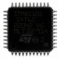
Manufacturer Part Number
STM8S105S4T6C
Description
MCU 16KB FLASH MEM 16MHZ 44LQFP
Manufacturer
STMicroelectronics
Series
STM8Sr
Datasheet
1.STM8S105C4T6.pdf
(127 pages)
Specifications of STM8S105S4T6C
Core Processor
STM8
Core Size
8-Bit
Speed
16MHz
Connectivity
I²C, IrDA, LIN, SPI, UART/USART
Peripherals
Brown-out Detect/Reset, POR, PWM, WDT
Number Of I /o
34
Program Memory Size
16KB (16K x 8)
Program Memory Type
FLASH
Eeprom Size
1K x 8
Ram Size
2K x 8
Voltage - Supply (vcc/vdd)
2.95 V ~ 5.5 V
Data Converters
A/D 9x10b
Oscillator Type
Internal
Operating Temperature
-40°C ~ 85°C
Package / Case
44-LQFP
Processor Series
STM8S10x
Core
STM8
Data Bus Width
8 bit
Data Ram Size
2 KB
Interface Type
I2C, SPI, UART
Maximum Clock Frequency
16 MHz
Number Of Programmable I/os
34
Number Of Timers
8
Maximum Operating Temperature
+ 85 C
Mounting Style
SMD/SMT
3rd Party Development Tools
EWSTM8
Development Tools By Supplier
STICE-SYS001
Minimum Operating Temperature
- 40 C
On-chip Adc
10 bit, 9 Channel
For Use With
497-10040 - EVAL KIT STM8S DISCOVERY497-10593 - KIT STARTER FOR STM8S207/8 SER497-5046 - KIT TOOL FOR ST7/UPSD/STR7 MCU
Lead Free Status / RoHS Status
Lead free / RoHS Compliant
Other names
497-8819
Available stocks
Company
Part Number
Manufacturer
Quantity
Price
Company:

Part Number:
STM8S105S4T6C
Manufacturer:
STMicroelectronics
Quantity:
10 000
Part Number:
STM8S105S4T6C
Manufacturer:
ST
Quantity:
20 000
Company:
Part Number:
STM8S105S4T6C
Manufacturer:
ST
Quantity:
18 870
Company:
Part Number:
STM8S105S4T6CTR
Manufacturer:
STMicroelectronics
Quantity:
10 000
Part Number:
STM8S105S4T6CTR
Manufacturer:
ST
Quantity:
20 000


List of figures
List of figures
Figure 1. STM8S105xx access line block diagram ................................................................................11
Figure 2. Flash memory organisation ....................................................................................................14
Figure 3. LQFP 48-pin pinout .................................................................................................................22
Figure 4. LQFP 44-pin pinout .................................................................................................................23
Figure 5. LQFP/VFQFPN/UFQFPN 32-pin pinout ................................................................................24
Figure 6. SDIP 32-pin pinout ..................................................................................................................25
Figure 7. Memory map ...........................................................................................................................30
Figure 8. Supply current measurement conditions ................................................................................56
Figure 9. Pin loading conditions .............................................................................................................57
Figure 10. Pin input voltage ...................................................................................................................57
Figure 11. f
Figure 12. External capacitor C
Figure 13. Typ. I
Figure 14. Typ. I
Figure 15. Typ. I
Figure 16. Typ. I
Figure 17. Typ. I
Figure 18. Typ. I
Figure 19. HSE external clocksource .....................................................................................................75
Figure 20. HSE oscillator circuit diagram ...............................................................................................76
Figure 21. Typical HSI accuracy at V
Figure 22. Typical HSI accuracy vs V
Figure 23. Typical LSI accuracy vs V
Figure 24. Typical V
Figure 25. Typical pull-up resistance vs V
Figure 26. Typical pull-up current vs V
Figure 27. Typ. V
Figure 28. Typ. V
Figure 29. Typ. V
Figure 30. Typ. V
Figure 31. Typ. V
Figure 32. Typ. V
Figure 33. Typ. V
Figure 34. Typ. V
Figure 35. Typ. V
Figure 36. Typ. V
Figure 37. Typical NRST V
Figure 38. Typical NRST pull-up resistance vs V
Figure 39. Typical NRST pull-up current vs V
Figure 40. Recommended reset pin protection ......................................................................................92
Figure 41. SPI timing diagram - slave mode and CPHA = 0 ..................................................................94
Figure 42. SPI timing diagram - slave mode and CPHA = 1
Figure 43. SPI timing diagram - master mode
Figure 44. Typical application with I
Figure 45. ADC accuracy characteristics .............................................................................................100
Figure 46. Typical application with ADC ..............................................................................................100
Figure 47. 48-pin low profile quad flat package (7 x 7) ........................................................................104
6/127
CPUmax
DD(RUN)
DD(RUN)
DD(WFI)
DD(WFI)
DD(WFI)
DD(RUN)
OL
OL
DD
DD
OL
OL
OL
OL
DD
DD
versus V
IL
@ V
@ V
@ V
@ V
- V
- V
@ V
@ V
- V
- V
and V
OH
OH
OH
OH
vs. V
vs. V
vs. f
vs. V
vs. f
vs. V
DD
DD
DD
DD
DD
DD
@ V
@ V
@ V
@ V
IL
= 5 V (true open drain ports) ......................................................................85
= 3.3 V (true open drain ports) ...................................................................86
= 5 V (high sink ports) ................................................................................86
= 3.3 V (high sink ports) .............................................................................87
= 5 V (standard ports) ................................................................................84
= 3.3 V (standard ports) .............................................................................85
DD
CPU
IH
CPU ,
DD ,
DD
and V
DD ,
DD ,
vs V
DD
DD
DD
DD
, HSI RC osc, f
EXT
, HSE user external clock V
HSE user external clock, f
..............................................................................................................61
HSE user external clock, f
HSI RC osc, f
= 5 V (standard ports) .......................................................................87
= 3.3 V (standard ports) ....................................................................88
HSE user external clock, V
= 5 V (high sink ports) ......................................................................88
= 3.3 V (high sink ports) ...................................................................89
DD
IH
2
C bus and timing diagram
DD
DD
.......................................................................................................62
DD
vs V
@ 4 temperatures ......................................................................81
DD
= 5 V vs 5 temperatures ..........................................................77
@ 4 temperatures ...................................................................79
@ 4 temperatures ..................................................................78
@ 4 temperatures .................................................................82
DD
DD
DocID14771 Rev 10
@ 4 temperatures ............................................................82
@ 4 temperatures ...........................................................90
DD
(1)
CPU
CPU
DD
@ 4 temperatures ......................................................91
...................................................................................95
= 16 MHz ................................................................74
@ 4 temperatures .................................................91
= 16 MHz ..............................................................72
CPU
DD
(1)
CPU
DD
= 5 V ....................................................73
= 16 MHz ............................................73
(1)
= 5 V ..................................................72
= 16 MHz ...........................................71
.............................................................94
.......................................................96
STM8S105xx
Related parts for STM8S105S4T6C
Image
Part Number
Description
Manufacturer
Datasheet
Request
R

Part Number:
Description:
EVAL KIT STM8S DISCOVERY
Manufacturer:
STMicroelectronics
Datasheet:

Part Number:
Description:
8 BITS MICROCONTR
Manufacturer:
STMicroelectronics
Datasheet:
Part Number:
Description:
8 BITS MICROCONTR
Manufacturer:
STMicroelectronics
Datasheet:

Part Number:
Description:
IC MCU 8BIT 128K FLASH 80-LQFP
Manufacturer:
STMicroelectronics
Datasheet:

Part Number:
Description:
MCU 32KB FLASH MEM 16MHZ 48-LQFP
Manufacturer:
STMicroelectronics
Datasheet:

Part Number:
Description:
MCU 8BIT 32K MEMORY 44-LQFP
Manufacturer:
STMicroelectronics
Datasheet:

Part Number:
Description:
MCU 8BIT 32K MEMORY 48-LQFP
Manufacturer:
STMicroelectronics
Datasheet:

Part Number:
Description:
MCU 8BIT 64K MEMORY 48-LQFP
Manufacturer:
STMicroelectronics
Datasheet:

Part Number:
Description:
MCU 8BIT 32K MEMORY 64-LQFP
Manufacturer:
STMicroelectronics
Datasheet:

Part Number:
Description:
MCU 8BIT 64K MEMORY 64-LQFP
Manufacturer:
STMicroelectronics
Datasheet:

Part Number:
Description:
IC MCU 8BIT 128K FLASH 64-LQFP
Manufacturer:
STMicroelectronics
Datasheet:

Part Number:
Description:
MCU 8BIT 128K MEMORY 64-LQFP
Manufacturer:
STMicroelectronics
Datasheet:
Part Number:
Description:
MCU 8BIT 8KB FLASH 20-TSSOP
Manufacturer:
STMicroelectronics
Datasheet:
Part Number:
Description:
MCU 8BIT 8KB FLASH 20-UFQFPN
Manufacturer:
STMicroelectronics
Datasheet:
Part Number:
Description:
MCU 8BIT 8KB FLASH 20-TSSOP
Manufacturer:
STMicroelectronics
Datasheet: