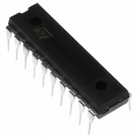
ST62T60CB6 STMicroelectronics, ST62T60CB6 Datasheet - Page 52

ST62T60CB6
Manufacturer Part Number
ST62T60CB6
Description
IC MCU 8BIT W/ADC 20-PDIP
Manufacturer
STMicroelectronics
Series
ST6r
Datasheet
1.ST62T60CB6.pdf
(83 pages)
Specifications of ST62T60CB6
Core Processor
ST6
Core Size
8-Bit
Speed
8MHz
Connectivity
SPI
Peripherals
LED, LVD, POR, WDT
Number Of I /o
13
Program Memory Size
3.8KB (3.8K x 8)
Program Memory Type
OTP
Eeprom Size
128 x 8
Ram Size
128 x 8
Voltage - Supply (vcc/vdd)
3 V ~ 6 V
Data Converters
A/D 7x8b
Oscillator Type
Internal
Operating Temperature
-40°C ~ 85°C
Package / Case
20-DIP (0.300", 7.62mm)
Processor Series
ST62T6x
Core
ST6
Data Bus Width
8 bit
Data Ram Size
128 B
Interface Type
SPI
Maximum Clock Frequency
8 MHz
Number Of Programmable I/os
13
Number Of Timers
2
Operating Supply Voltage
3 V to 6 V
Maximum Operating Temperature
+ 85 C
Mounting Style
Through Hole
Development Tools By Supplier
ST622XC-KIT/110, ST62GP-EMU2, ST62E2XC-EPB/110, ST62E6XC-EPB/US, STREALIZER-II
Minimum Operating Temperature
- 40 C
On-chip Adc
7-ch x 8-bit
Controller Family/series
ST6
No. Of I/o's
13
Eeprom Memory Size
128Byte
Ram Memory Size
128Byte
Cpu Speed
8MHz
No. Of Timers
2
Rohs Compliant
Yes
Lead Free Status / RoHS Status
Lead free / RoHS Compliant
Available stocks
Company
Part Number
Manufacturer
Quantity
Price
Company:
Part Number:
ST62T60CB6
Manufacturer:
ST
Quantity:
415
Company:
Part Number:
ST62T60CB6
Manufacturer:
STMicroelectronics
Quantity:
1 820
Part Number:
ST62T60CB6
Manufacturer:
ST
Quantity:
20 000
A/D CONVERTER (Cont’d)
Since the ADC is on the same chip as the micro-
processor, the user should not switch heavily load-
ed output signals during conversion, if high preci-
sion is required. Such switching will affect the sup-
ply voltages used as analog references.
The accuracy of the conversion depends on the
quality of the power supplies (V
user must take special care to ensure a well regu-
lated reference voltage is present on the V
V
less than 5V/ms). This implies, in particular, that a
suitable decoupling capacitor is used at the V
pin.
The converter resolution is given by::
The Input voltage (Ain) which is to be converted
must be constant for 1µs before conversion and
remain constant during conversion.
Conversion resolution can be improved if the pow-
er supply voltage (V
lowered.
In order to optimise conversion resolution, the user
can configure the microcontroller in WAIT mode,
because this mode minimises noise disturbances
and power supply variations due to output switch-
ing. Nevertheless, the WAIT instruction should be
executed as soon as possible after the beginning
of the conversion, because execution of the WAIT
instruction may cause a small variation of the V
voltage. The negative effect of this variation is min-
imized at the beginning of the conversion when the
converter is less sensitive, rather than at the end
of conversion, when the less significant bits are
determined.
The best configuration, from an accuracy stand-
point, is WAIT mode with the Timer stopped. In-
deed, only the ADC peripheral and the oscillator
are then still working. The MCU must be woken up
from WAIT mode by the ADC interrupt at the end
of the conversion. It should be noted that waking
up the microcontroller could also be done using
the Timer interrupt, but in this case the Timer will
be working and the resulting noise could affect
conversion accuracy.
One extra feature is available in the ADC to get a
better accuracy. In fact, each ADC conversion has
to be followed by a WAIT instruction to minimize
SS
pins (power supply voltage variations must be
V
--------------------------- -
DD
DD
256
) to the microcontroller is
–
V
SS
DD
and V
SS
DD
). The
and
DD
DD
ST6253C ST6263C ST6263B ST6260C ST6260B
the noise during the conversion. But the first con-
version step is performed before the execution of
the WAIT when most of clocks signals are still en-
abled . The key is to synchronize the ADC start
with the effective execution of the WAIT. This is
achieved by setting ADC SYNC option. This way,
ADC conversion starts in effective WAIT for maxi-
mum accuracy.
Note: With this extra option, it is mandatory to ex-
ecute WAIT instruction just after ADC start instruc-
tion. Insertion of any extra instruction may cause
spurious interrupt request at ADC interrupt vector.
A/D Converter Control Register (ADCR)
Address: 0D1h — Read/Write
Bit 7 = EAI: Enable A/D Interrupt. If this bit is set to
“1” the A/D interrupt is enabled, when EAI=0 the
interrupt is disabled.
Bit 6 = EOC: End of conversion. Read Only. This
read only bit indicates when a conversion has
been completed. This bit is automatically reset to
“0” when the STA bit is written. If the user is using
the interrupt option then this bit can be used as an
interrupt pending bit. Data in the data conversion
register are valid only when this bit is set to “1”.
Bit 5 = STA: Start of Conversion. Write Only. Writ-
ing a “1” to this bit will start a conversion on the se-
lected channel and automatically reset to “0” the
EOC bit. If the bit is set again when a conversion is
in progress, the present conversion is stopped and
a new one will take place. This bit is write only, any
attempt to read it will show a logical zero.
Bit 4 = PDS: Power Down Selection. This bit acti-
vates the A/D converter if set to “1”. Writing a “0” to
this bit will put the ADC in power down mode (idle
mode).
Bit 3-0 = D3-D0. Not used
A/D Converter Data Register (ADR)
Address: 0D0h — Read only
Bit 7-0 = D7-D0: 8 Bit A/D Conversion Result.
EAI
D7
7
7
EOC
D6
STA
D5
PDS
D4
D3
D3
D2
D2
D1
D1
52/83
D0
D0
0
0


