STM32F103C6T7A STMicroelectronics, STM32F103C6T7A Datasheet - Page 15
STM32F103C6T7A
Manufacturer Part Number
STM32F103C6T7A
Description
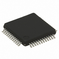
MCU ARM 32BIT 32KB FLASH 48LQFP
Manufacturer
STMicroelectronics
Series
STM32r
Specifications of STM32F103C6T7A
Core Processor
ARM® Cortex-M3™
Core Size
32-Bit
Speed
72MHz
Connectivity
CAN, I²C, IrDA, LIN, SPI, UART/USART, USB
Peripherals
DMA, Motor Control PWM, PDR, POR, PVD, PWM, Temp Sensor, WDT
Number Of I /o
37
Program Memory Size
32KB (32K x 8)
Program Memory Type
FLASH
Ram Size
10K x 8
Voltage - Supply (vcc/vdd)
2 V ~ 3.6 V
Data Converters
A/D 10x12b
Oscillator Type
Internal
Operating Temperature
-40°C ~ 105°C
Package / Case
48-LQFP
Featured Product
STM32 Cortex-M3 Companion Products
Eeprom Size
-
Cpu Family
STM32
Device Core
ARM Cortex-M3
Device Core Size
32b
Frequency (max)
72MHz
Interface Type
CAN/I2C/SPI/USART
Total Internal Ram Size
10KB
# I/os (max)
37
Number Of Timers - General Purpose
3
Operating Supply Voltage (typ)
2.5/3.3V
Operating Supply Voltage (max)
3.6V
Operating Supply Voltage (min)
2V
On-chip Adc
2(10-chx12-bit)
Instruction Set Architecture
RISC
Operating Temp Range
-40C to 105C
Operating Temperature Classification
Industrial
Mounting
Surface Mount
Pin Count
48
Package Type
LQFP
For Use With
497-10048 - BOARD EVAL ACCELEROMETER497-10030 - STARTER KIT FOR STM32KSDKSTM32-PL - KIT IAR KICKSTART STM32 CORTEXM3497-8512 - KIT STARTER FOR STM32F10XE MCU497-8511 - KIT STARTER FOR STM32 512K FLASH497-8505 - KIT STARTER FOR STM32F10XE MCU497-6438 - BOARD EVALUTION FOR STM32 512K497-6289 - KIT PERFORMANCE STICK FOR STM32MCBSTM32UME - BOARD EVAL MCBSTM32 + ULINK-MEMCBSTM32U - BOARD EVAL MCBSTM32 + ULINK2MCBSTM32 - BOARD EVAL FOR STM STM32X SER497-6053 - KIT STARTER FOR STM32497-6052 - KIT STARTER FOR STM32497-6050 - KIT STARTER FOR STM32497-6049 - KIT EVALUATION LOW COST STM32497-6048 - BOARD EVALUATION FOR STM32497-6047 - KIT DEVELOPMENT FOR STM32
Lead Free Status / RoHS Status
Lead free / RoHS Compliant
Eeprom Size
-
Lead Free Status / Rohs Status
Lead free / RoHS Compliant
Available stocks
Company
Part Number
Manufacturer
Quantity
Price
Company:

Part Number:
STM32F103C6T7A
Manufacturer:
ST
Quantity:
1 500
Company:
Part Number:
STM32F103C6T7A
Manufacturer:
STMicroelectronics
Quantity:
10 000
Part Number:
STM32F103C6T7A
Manufacturer:
ST
Quantity:
20 000
Company:
Part Number:
STM32F103C6T7ATR
Manufacturer:
STMicroelectronics
Quantity:
10 000


STM32F103x4, STM32F103x6
2.3.6
2.3.7
2.3.8
2.3.9
2.3.10
This hardware block provides flexible interrupt management features with minimal interrupt
latency.
External interrupt/event controller (EXTI)
The external interrupt/event controller consists of 19 edge detector lines used to generate
interrupt/event requests. Each line can be independently configured to select the trigger
event (rising edge, falling edge, both) and can be masked independently. A pending register
maintains the status of the interrupt requests. The EXTI can detect an external line with a
pulse width shorter than the Internal APB2 clock period. Up to 51 GPIOs can be connected
to the 16 external interrupt lines.
Clocks and startup
System clock selection is performed on startup, however the internal RC 8 MHz oscillator is
selected as default CPU clock on reset. An external 4-16 MHz clock can be selected, in
which case it is monitored for failure. If failure is detected, the system automatically switches
back to the internal RC oscillator. A software interrupt is generated if enabled. Similarly, full
interrupt management of the PLL clock entry is available when necessary (for example on
failure of an indirectly used external crystal, resonator or oscillator).
Several prescalers allow the configuration of the AHB frequency, the high-speed APB
(APB2) and the low-speed APB (APB1) domains. The maximum frequency of the AHB and
the high-speed APB domains is 72 MHz. The maximum allowed frequency of the low-speed
APB domain is 36 MHz. See
Boot modes
At startup, boot pins are used to select one of three boot options:
●
●
●
The boot loader is located in System Memory. It is used to reprogram the Flash memory by
using USART1. For further details please refer to AN2606.
Power supply schemes
●
●
●
For more details on how to connect power pins, refer to
Power supply supervisor
The device has an integrated power-on reset (POR)/power-down reset (PDR) circuitry. It is
always active, and ensures proper operation starting from/down to 2 V. The device remains
Boot from User Flash
Boot from System Memory
Boot from embedded SRAM
V
Provided externally through V
V
and PLL (minimum voltage to be applied to V
V
V
registers (through power switch) when V
DD
SSA
DDA
BAT
= 2.0 to 3.6 V: external power supply for I/Os and the internal regulator.
, V
= 1.8 to 3.6 V: power supply for RTC, external clock 32 kHz oscillator and backup
and V
DDA
SSA
= 2.0 to 3.6 V: external analog power supplies for ADC, reset blocks, RCs
must be connected to V
Figure 2
Doc ID 15060 Rev 5
DD
pins.
for details on the clock tree.
DD
DD
and V
is not present.
DDA
SS
is 2.4 V when the ADC is used).
Figure 11: Power supply
, respectively.
Description
scheme.
15/87
Related parts for STM32F103C6T7A
Image
Part Number
Description
Manufacturer
Datasheet
Request
R

Part Number:
Description:
STMicroelectronics [RIPPLE-CARRY BINARY COUNTER/DIVIDERS]
Manufacturer:
STMicroelectronics
Datasheet:
Part Number:
Description:
STMicroelectronics [LIQUID-CRYSTAL DISPLAY DRIVERS]
Manufacturer:
STMicroelectronics
Datasheet:

Part Number:
Description:
BOARD EVAL FOR MEMS SENSORS
Manufacturer:
STMicroelectronics
Datasheet:
Part Number:
Description:
NPN TRANSISTOR POWER MODULE
Manufacturer:
STMicroelectronics
Datasheet:
Part Number:
Description:
TURBOSWITCH ULTRA-FAST HIGH VOLTAGE DIODE
Manufacturer:
STMicroelectronics
Datasheet:
Part Number:
Description:
Manufacturer:
STMicroelectronics
Datasheet:
Part Number:
Description:
DIODE / SCR MODULE
Manufacturer:
STMicroelectronics
Datasheet:
Part Number:
Description:
DIODE / SCR MODULE
Manufacturer:
STMicroelectronics
Datasheet:
Part Number:
Description:
Search -----> STE16N100
Manufacturer:
STMicroelectronics
Datasheet:
Part Number:
Description:
Search ---> STE53NA50
Manufacturer:
STMicroelectronics
Datasheet:
Part Number:
Description:
NPN Transistor Power Module
Manufacturer:
STMicroelectronics
Datasheet:
Part Number:
Description:
DIODE / SCR MODULE
Manufacturer:
STMicroelectronics
Datasheet: