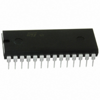
ST62T65CB6 STMicroelectronics, ST62T65CB6 Datasheet - Page 53

ST62T65CB6
Manufacturer Part Number
ST62T65CB6
Description
IC MCU 8BIT W/ADC 28-PDIP
Manufacturer
STMicroelectronics
Series
ST6r
Datasheet
1.ST62T55CB6.pdf
(84 pages)
Specifications of ST62T65CB6
Core Processor
ST6
Core Size
8-Bit
Speed
8MHz
Connectivity
SPI
Peripherals
LED, LVD, POR, WDT
Number Of I /o
21
Program Memory Size
3.8KB (3.8K x 8)
Program Memory Type
OTP
Eeprom Size
128 x 8
Ram Size
128 x 8
Voltage - Supply (vcc/vdd)
3 V ~ 6 V
Data Converters
A/D 13x8b
Oscillator Type
Internal
Operating Temperature
-40°C ~ 85°C
Package / Case
28-DIP (0.600", 15.24mm)
Processor Series
ST62T6x
Core
ST6
Data Bus Width
8 bit
Data Ram Size
128 B
Interface Type
SCI
Maximum Clock Frequency
8 MHz
Number Of Programmable I/os
21
Number Of Timers
1
Operating Supply Voltage
3 V to 6 V
Maximum Operating Temperature
+ 125 C
Mounting Style
Through Hole
Development Tools By Supplier
ST62GP-EMU2, ST62E2XC-EPB/110, ST62E6XC-EPB/US, STREALIZER-II
Minimum Operating Temperature
- 40 C
On-chip Adc
8 bit
Lead Free Status / RoHS Status
Lead free / RoHS Compliant
Available stocks
Company
Part Number
Manufacturer
Quantity
Price
Company:
Part Number:
ST62T65CB6
Manufacturer:
BOURNS
Quantity:
12 000
4.5 SERIAL PERIPHERAL INTERFACE (SPI)
The SPI peripheral is an optimized synchronous
serial interface with programmable transmission
modes and master/slave capabilities supporting a
wide range of industry standard SPI specifications.
The SPI interface may also implement asynchro-
nous data transfer, in which case processor over-
head is limited to data transfer from or to the shift
register on an interrupt driven basis.
The SPI may be controlled by simple user soft-
ware to perform serial data exchange with low-
cost external memory, or with serially controlled
peripherals to drive displays, motors or relays.
The SPI’s shift register is simultaneously fed by
the Sin pin and feeds the Sout pin, thus transmis-
sion and reception are essentially the same proc-
ess. Suitable setting of the number of bits in the
data frame can allow filtering of unwanted leading
data bits in the incoming data stream.
The SPI comprises an 8-bit Data/Shift Register,
DSR, a Divide register, DIV, a Mode Control Reg-
ister MOD, and a Miscellaneous register, MISCR.
The SPI may be operated either in Master mode or
in Slave mode.
Master mode is defined by the synchronous serial
clock being supplied by the MCU, by suitably pro-
gramming the clock divider (DIV register). Slave
Figure 30. SPI Block Diagram
SCK
CLOCK
Sin
CYCLE
CPU
DIVIDER
SPI
FILTER
FILTER
mode is defined by the serial clock being supplied
externally on the SCK pin by the external Master
device.
For maximum versatility the SPI may be pro-
grammed to sample data either on the rising or on
the falling edge of SCK, with or without phase shift
(clock Polarity and Phase selection).
The Sin, Sout and SCK signals are connected as
alternate I/O pin functions.
For serial input operation, Sin must be configured
as an input. For serial output operation, Sout is se-
lected as an output by programming Bit 0 of the
Miscellaneous Register: clearing this bit will set
the pin as a standard I/O line, while setting the bit
will select the Sout function.
An interrupt request may be associated with the
end of a transmission or reception cycle; this is de-
fined by programming the number of bits in the
data frame and by enabling the interrupt. This re-
quest is associated with interrupt vector #2, and
can be masked by programming the SPIE bit of
the MOD register. Since the SPI interrupt is
“ORed” with the port interrupt source, an interrupt
flag bit is available in the DIV register allowing dis-
crimination of the interrupt request.
DATA BUS
8
ST6255C ST6265C ST6265B
CLOCK
REGISTER
SHIFT
VR001693
Sout
53/84


