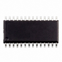
ST62T65CM6 STMicroelectronics, ST62T65CM6 Datasheet - Page 8

ST62T65CM6
Manufacturer Part Number
ST62T65CM6
Description
IC MCU 8BIT OTP/EPROM 28 PSOIC
Manufacturer
STMicroelectronics
Series
ST6r
Datasheet
1.ST62T55CB6.pdf
(84 pages)
Specifications of ST62T65CM6
Core Processor
ST6
Core Size
8-Bit
Speed
8MHz
Connectivity
SPI
Peripherals
LED, LVD, POR, WDT
Number Of I /o
21
Program Memory Size
3.8KB (3.8K x 8)
Program Memory Type
OTP
Eeprom Size
128 x 8
Ram Size
128 x 8
Voltage - Supply (vcc/vdd)
3 V ~ 6 V
Data Converters
A/D 13x8b
Oscillator Type
Internal
Operating Temperature
-40°C ~ 85°C
Package / Case
28-SOIC (7.5mm Width)
Controller Family/series
ST6
No. Of I/o's
21
Eeprom Memory Size
128Byte
Ram Memory Size
128Byte
Cpu Speed
8MHz
No. Of Timers
2
Rohs Compliant
Yes
Processor Series
ST62T6x
Core
ST6
Data Bus Width
8 bit
Data Ram Size
128 B
Interface Type
SCI
Maximum Clock Frequency
8 MHz
Number Of Programmable I/os
21
Number Of Timers
1
Operating Supply Voltage
3 V to 6 V
Maximum Operating Temperature
+ 125 C
Mounting Style
SMD/SMT
Development Tools By Supplier
ST62GP-EMU2, ST62E2XC-EPB/110, ST62E6XC-EPB/US, STREALIZER-II
Minimum Operating Temperature
- 40 C
On-chip Adc
8 bit
Lead Free Status / RoHS Status
Lead free / RoHS Compliant
Other names
497-2103-5
Available stocks
Company
Part Number
Manufacturer
Quantity
Price
Company:
Part Number:
ST62T65CM6
Manufacturer:
ST
Quantity:
700
ST6255C ST6265C ST6265B
MEMORY MAP (Cont’d)
1.3.5 Data Window Register (DWR)
The Data read-only memory window is located from
address 0040h to address 007Fh in Data space. It
allows direct reading of 64 consecutive bytes locat-
ed anywhere in program memory, between ad-
dress 0000h and 0FFFh (top memory address de-
pends on the specific device). All the program
memory can therefore be used to store either in-
structions or read-only data. Indeed, the window
can be moved in steps of 64 bytes along the pro-
gram memory by writing the appropriate code in the
Data Window Register (DWR).
The DWR can be addressed like any RAM location
in the Data Space, it is however a write-only regis-
ter and therefore cannot be accessed using single-
bit operations. This register is used to position the
64-byte read-only data window (from address 40h
to address 7Fh of the Data space) in program
memory in 64-byte steps. The effective address of
the byte to be read as data in program memory is
obtained by concatenating the 6 least significant
bits of the register address given in the instruction
(as least significant bits) and the content of the
DWR register (as most significant bits), as illustrat-
ed in
ing location 0040h of the Data Space, with 0 load-
ed in the DWR register, the physical location ad-
dressed in program memory is 00h. The DWR reg-
ister is not cleared on reset, therefore it must be
written to prior to the first access to the Data read-
only memory window area.
Figure 5. Data read-only memory Window Memory Addressing
8/84
WINDOW REGISTER
Figure 5
ADDRESS:A19h
CONTENTS
DATA ROM
(DWR)
Example:
DWR=28h
ROM
below. For instance, when address-
13
7
12
6
11
5
1
1
10
4
0
0
9
3
1
1
8
2
0
0
7
1
0
0
0
0
6
0
1
0
1
0
5
5
0
0
Data Window Register (DWR)
Address: 0C9h — Write Only
Bits 6, 7 = Not used.
Bit 5-0 = DWR5-DWR0: Data read-only memory
Window Register Bits. These are the Data read-
only memory Window bits that correspond to the
upper bits of the data read-only memory space.
Caution: This register is undefined on reset. Nei-
ther read nor single bit instructions may be used to
address this register.
Note: Care is required when handling the DWR
register as it is write only. For this reason, the
DWR contents should not be changed while exe-
cuting an interrupt service routine, as the service
routine cannot save and then restore the register’s
previous contents. If it is impossible to avoid writ-
ing to the DWR during the interrupt service routine,
an image of the register must be saved in a RAM
location, and each time the program writes to the
DWR, it must also write to the image register. The
image register must be written first so that, if an in-
terrupt occurs between the two instructions, the
DWR is not affected.
7
4
4
-
1
1
3
3
1
1
-
2
2
0
0
DWR5 DWR4 DWR3 DWR2 DWR1 DWR0
1
1
0
0
0
0
1
1
PROGRAM SPACE ADDRESS
DATA SPACE ADDRESS
DATA SPACE ADDRESS
IN INSTRUCTION
40h-7Fh
READ
59h
VR01573C
:
:
0


