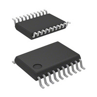
R5F21324CNSP#U0 Renesas Electronics America, R5F21324CNSP#U0 Datasheet - Page 379

R5F21324CNSP#U0
Manufacturer Part Number
R5F21324CNSP#U0
Description
MCU 1KB FLASH 16K ROM 20-LSSOP
Manufacturer
Renesas Electronics America
Series
R8C/3x/32Cr
Datasheet
1.R5F21321CDSPU0.pdf
(605 pages)
Specifications of R5F21324CNSP#U0
Core Processor
R8C
Core Size
16/32-Bit
Speed
20MHz
Connectivity
I²C, LIN, SIO, SSU, UART/USART
Peripherals
POR, PWM, Voltage Detect, WDT
Number Of I /o
15
Program Memory Size
16KB (16K x 8)
Program Memory Type
FLASH
Ram Size
1.5K x 8
Voltage - Supply (vcc/vdd)
1.8 V ~ 5.5 V
Data Converters
A/D 4x10b
Oscillator Type
Internal
Operating Temperature
-20°C ~ 85°C
Package / Case
20-LSSOP
Lead Free Status / RoHS Status
Lead free / RoHS Compliant
Eeprom Size
-
- Current page: 379 of 605
- Download datasheet (6Mb)
R8C/32C Group
REJ09B0573-0100 Rev.1.00 Dec. 18, 2009
Page 350 of 573
22.5.5
22.5.6
22.5.7
When the IICM2 bit is set to 0, the 1st to 8th bits (D7 to D0) of received data are stored in bits b7 to b0 in the
U2RB register. The 9th bit (D8) is ACK or NACK.
When the IICM2 bit is set to 1, the 1st to 7th bits (D7 to D1) of received data are stored in bits b6 to b0 in the
U2RB register and the 8th bit (D0) is stored in bit b8 in the U2RB register. Even when the IICM2 bit is set to 1,
if the CKPH bit is 1, the same data as when the IICM2 bit is 0 can be read by reading the U2RB register after
the rising edge of 9th bit of the clock.
If the STSPSEL bit in the U2SMR4 register is set to 0 (start and stop conditions not output) and the ACKC bit
in the U2SMR4 register is set to 1 (ACK data output), the value of the ACKD bit in the U2SMR4 register is
output from the SDA2 pin.
If the IICM2 bit is set to 0, a NACK interrupt request is generated if the SDA2 pin remains high at the rising
edge of the 9th bit of transmit clock pulse. An ACK interrupt request is generated if the SDA2 pin is low at the
rising edge of the 9th bit of the transmit clock.
If ACK2 (UART2 reception) is selected to generate a DTC request source, a DTC transfer can be activated by
detection of an acknowledge.
If a start condition is detected while the STAC bit is set to 1 (UART2 initialization enabled), the serial interface
operates as described below.
• The transmit shift register is initialized, and the contents of the U2TB register are transferred to the transmit
• The receive shift register is initialized, and the serial interface starts receiving data when the next clock pulse
• The SWC bit is set to 1 (SCL wait output enabled). Consequently, the SCL2 pin is pulled low at the falling
Note that when UART2 transmission/reception is started using this function, the TI bit does not change state.
Select the external clock as the transfer clock to start UART2 transmission/reception with this setting.
shift register. In this way, the serial interface starts sending data when the next clock pulse is applied.
However, the UART2 output value does not change state and remains the same as when a start condition was
detected until the first bit of data is output in synchronization with the input clock.
is applied.
edge of the 9th clock pulse.
SDA Input
ACK and NACK
Initialization of Transmission/Reception
22. Serial Interface (UART2)
Related parts for R5F21324CNSP#U0
Image
Part Number
Description
Manufacturer
Datasheet
Request
R

Part Number:
Description:
KIT STARTER FOR M16C/29
Manufacturer:
Renesas Electronics America
Datasheet:

Part Number:
Description:
KIT STARTER FOR R8C/2D
Manufacturer:
Renesas Electronics America
Datasheet:

Part Number:
Description:
R0K33062P STARTER KIT
Manufacturer:
Renesas Electronics America
Datasheet:

Part Number:
Description:
KIT STARTER FOR R8C/23 E8A
Manufacturer:
Renesas Electronics America
Datasheet:

Part Number:
Description:
KIT STARTER FOR R8C/25
Manufacturer:
Renesas Electronics America
Datasheet:

Part Number:
Description:
KIT STARTER H8S2456 SHARPE DSPLY
Manufacturer:
Renesas Electronics America
Datasheet:

Part Number:
Description:
KIT STARTER FOR R8C38C
Manufacturer:
Renesas Electronics America
Datasheet:

Part Number:
Description:
KIT STARTER FOR R8C35C
Manufacturer:
Renesas Electronics America
Datasheet:

Part Number:
Description:
KIT STARTER FOR R8CL3AC+LCD APPS
Manufacturer:
Renesas Electronics America
Datasheet:

Part Number:
Description:
KIT STARTER FOR RX610
Manufacturer:
Renesas Electronics America
Datasheet:

Part Number:
Description:
KIT STARTER FOR R32C/118
Manufacturer:
Renesas Electronics America
Datasheet:

Part Number:
Description:
KIT DEV RSK-R8C/26-29
Manufacturer:
Renesas Electronics America
Datasheet:

Part Number:
Description:
KIT STARTER FOR SH7124
Manufacturer:
Renesas Electronics America
Datasheet:

Part Number:
Description:
KIT STARTER FOR H8SX/1622
Manufacturer:
Renesas Electronics America
Datasheet:

Part Number:
Description:
KIT DEV FOR SH7203
Manufacturer:
Renesas Electronics America
Datasheet:


