MC908LJ24CFUER Freescale Semiconductor, MC908LJ24CFUER Datasheet - Page 327
MC908LJ24CFUER
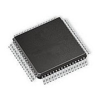
Manufacturer Part Number
MC908LJ24CFUER
Description
IC MCU 24K FLASH 8MHZ SPI 64-QFP
Manufacturer
Freescale Semiconductor
Series
HC08r
Datasheet
1.MC908LK24CFUE.pdf
(464 pages)
Specifications of MC908LJ24CFUER
Core Processor
HC08
Core Size
8-Bit
Speed
8MHz
Connectivity
I²C, IRSCI, SPI
Peripherals
LCD, LVD, POR, PWM
Number Of I /o
40
Program Memory Size
24KB (24K x 8)
Program Memory Type
FLASH
Ram Size
768 x 8
Voltage - Supply (vcc/vdd)
3 V ~ 5.5 V
Data Converters
A/D 6x10b
Oscillator Type
Internal
Operating Temperature
-40°C ~ 85°C
Package / Case
64-QFP
Processor Series
HC08LJ
Core
HC08
Data Bus Width
8 bit
Data Ram Size
768 B
Interface Type
SCI, SPI
Maximum Clock Frequency
8 MHz
Number Of Programmable I/os
48
Number Of Timers
4
Maximum Operating Temperature
+ 85 C
Mounting Style
SMD/SMT
Development Tools By Supplier
FSICEBASE, M68EML08LJLKE, ZK-HC08LX-A, M68CBL05CE
Minimum Operating Temperature
- 40 C
On-chip Adc
10 bit, 6 Channel
Lead Free Status / RoHS Status
Lead free / RoHS Compliant
Eeprom Size
-
Lead Free Status / Rohs Status
Details
Available stocks
Company
Part Number
Manufacturer
Quantity
Price
Company:

Part Number:
MC908LJ24CFUER
Manufacturer:
Freescale Semiconductor
Quantity:
10 000


MC68HC908LJ24/LK24 — Rev. 2.1
Freescale Semiconductor
MMTXIF — Multi-Master Transmit Interrupt Flag
MMATCH — Multi-Master Address Match
MMSRW — Multi-Master Slave Read/Write
MMRXAK — Multi-Master Receive Acknowledge
This flag is set when data in the data transmit register (MMDTR) is
downloaded to the output circuit, and that new data can be written to
the MMDTR. MMTXIF generates an interrupt request to CPU if the
MMIEN bit in MMCR is also set. This bit is cleared by writing "0" to it
or when the MMEN = 0.
This flag is set when the received data in the data receive register
(MMDRR) is an calling address which matches with the address or its
extended addresses (MMEXTAD=1) specified in the MMADR
register.
This bit indicates the data direction when the module is in slave mode.
It is updated after the calling address is received from a master
device. MMSRW = 1 when the calling master is reading data from the
module (slave transmit mode). MMSRW = 0 when the master is
writing data to the module (receive mode).
When this bit is cleared, it indicates an acknowledge signal has been
received after the completion of 8 data bits transmission on the bus.
When MMRXAK is set, it indicates no acknowledge signal has been
detected at the 9th clock; the module will release the SDA line for the
master to generate "stop" or "repeated start" condition. Reset sets this
bit.
1 = Data transfer completed
0 = Data transfer in progress
1 = Received address matches MMADR
0 = Received address does not match
1 = Slave mode transmit
0 = Slave mode receive
1 = No acknowledge signal received at 9th clock bit
0 = Acknowledge signal received at 9th clock bit
Multi-Master IIC Interface (MMIIC)
Multi-Master IIC Interface (MMIIC)
Multi-Master IIC Registers
Data Sheet
327
Related parts for MC908LJ24CFUER
Image
Part Number
Description
Manufacturer
Datasheet
Request
R

Part Number:
Description:
Manufacturer:
Freescale Semiconductor, Inc
Datasheet:
Part Number:
Description:
Manufacturer:
Freescale Semiconductor, Inc
Datasheet:
Part Number:
Description:
Manufacturer:
Freescale Semiconductor, Inc
Datasheet:
Part Number:
Description:
Manufacturer:
Freescale Semiconductor, Inc
Datasheet:
Part Number:
Description:
Manufacturer:
Freescale Semiconductor, Inc
Datasheet:
Part Number:
Description:
Manufacturer:
Freescale Semiconductor, Inc
Datasheet:
Part Number:
Description:
Manufacturer:
Freescale Semiconductor, Inc
Datasheet:
Part Number:
Description:
Manufacturer:
Freescale Semiconductor, Inc
Datasheet:
Part Number:
Description:
Manufacturer:
Freescale Semiconductor, Inc
Datasheet:
Part Number:
Description:
Manufacturer:
Freescale Semiconductor, Inc
Datasheet:
Part Number:
Description:
Manufacturer:
Freescale Semiconductor, Inc
Datasheet:
Part Number:
Description:
Manufacturer:
Freescale Semiconductor, Inc
Datasheet:
Part Number:
Description:
Manufacturer:
Freescale Semiconductor, Inc
Datasheet:
Part Number:
Description:
Manufacturer:
Freescale Semiconductor, Inc
Datasheet:
Part Number:
Description:
Manufacturer:
Freescale Semiconductor, Inc
Datasheet: