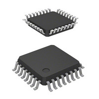
R5F21334CNFP#U0 Renesas Electronics America, R5F21334CNFP#U0 Datasheet - Page 216

R5F21334CNFP#U0
Manufacturer Part Number
R5F21334CNFP#U0
Description
MCU 1KB FLASH 16K ROM 32-LQFP
Manufacturer
Renesas Electronics America
Series
R8C/3x/33Cr
Datasheet
1.R5F21331CNFPU0.pdf
(622 pages)
Specifications of R5F21334CNFP#U0
Core Processor
R8C
Core Size
16/32-Bit
Speed
20MHz
Connectivity
I²C, LIN, SIO, SSU, UART/USART
Peripherals
POR, PWM, Voltage Detect, WDT
Number Of I /o
27
Program Memory Size
16KB (16K x 8)
Program Memory Type
FLASH
Ram Size
1.5K x 8
Voltage - Supply (vcc/vdd)
1.8 V ~ 5.5 V
Data Converters
A/D 12x10b; D/A 2x8b
Oscillator Type
Internal
Operating Temperature
-20°C ~ 85°C
Package / Case
32-LQFP
Lead Free Status / RoHS Status
Lead free / RoHS Compliant
Eeprom Size
-
Available stocks
Company
Part Number
Manufacturer
Quantity
Price
Part Number:
R5F21334CNFP#U0R5F21334CNFP#V2
Manufacturer:
Renesas Electronics America
Quantity:
10 000
- Current page: 216 of 622
- Download datasheet (7Mb)
R8C/33C Group
REJ09B0570-0100 Rev.1.00 Dec. 14, 2009
Page 186 of 589
Figure 15.3
Figure 15.4
Write 0 to the interrupt source
flag in the status register
Write back control data
Write back control data
DTC activation source
DTC activation source
Read control data
Read control data
Read DTC vector
Read DTC vector
Transfer data
Transfer data
generation
NMIF = 1?
generation
CHNE=1?
NMIF = 1?
CHNE=1?
Branch 1
Branch 1
End
End
No
No
No
No
Timer RC, or Flash Memory Interrupt Source
Source
DTC Internal Operation Flowchart When DTC Activation Source is not SSU/I
DTC Internal Operation Flowchart When DTC Activation Source is Timer RC Interrupt
Yes
Yes
Yes
Yes
Write back control data
Write back control data
Read control data
Read control data
Transfer data
Transfer data
CHNE=1?
CHNE=1?
No
No
Yes
Yes
Branch 1
0 is written to the bit among bits DTCENi0 to DTCENi7 and an interrupt request is generated
when transfer is either of the following:
- Transfer causing the DTCCTj (j = 0 to 23) register value to change from 1 to 0 in normal mode
- Transfer causing the DTCCTj register value to change from 1 to 0 while the RPTINT bit is 1 in
DTCENi0 to DTCENi7: Bits in DTCENi (i = 0 to 3, 5, 6) registers
RPTINT, CHNE: Bits in DTCCRj registers
NMIF: Bit in DTCTL register
DTCENi0 to DTCENi7: Bits in DTCENi (i = 0 to 3, 5, 6) registers
RPTINT, CHNE: Bits in DTCCRj registers
NMIF: Bit in DTCTL register
repeat mode
repeat mode
Generate an interrupt request
Generate an interrupt request
Write 0 to the bit among
Write 0 to the bit among
Write back control data
Write back control data
DTCENi0 to DTCENi7
DTCENi0 to DTCENi7
Interrupt handling
Interrupt handling
Transfer data
Transfer data
for the CPU
for the CPU
CHNE=1?
CHNE=1?
No
No
Yes
Yes
Write back control data
Write back control data
Read control data
Read control data
Transfer data
Transfer data
CHNE=1?
CHNE=1?
No
No
Yes
Yes
2
C bus,
15. DTC
Related parts for R5F21334CNFP#U0
Image
Part Number
Description
Manufacturer
Datasheet
Request
R

Part Number:
Description:
KIT STARTER FOR M16C/29
Manufacturer:
Renesas Electronics America
Datasheet:

Part Number:
Description:
KIT STARTER FOR R8C/2D
Manufacturer:
Renesas Electronics America
Datasheet:

Part Number:
Description:
R0K33062P STARTER KIT
Manufacturer:
Renesas Electronics America
Datasheet:

Part Number:
Description:
KIT STARTER FOR R8C/23 E8A
Manufacturer:
Renesas Electronics America
Datasheet:

Part Number:
Description:
KIT STARTER FOR R8C/25
Manufacturer:
Renesas Electronics America
Datasheet:

Part Number:
Description:
KIT STARTER H8S2456 SHARPE DSPLY
Manufacturer:
Renesas Electronics America
Datasheet:

Part Number:
Description:
KIT STARTER FOR R8C38C
Manufacturer:
Renesas Electronics America
Datasheet:

Part Number:
Description:
KIT STARTER FOR R8C35C
Manufacturer:
Renesas Electronics America
Datasheet:

Part Number:
Description:
KIT STARTER FOR R8CL3AC+LCD APPS
Manufacturer:
Renesas Electronics America
Datasheet:

Part Number:
Description:
KIT STARTER FOR RX610
Manufacturer:
Renesas Electronics America
Datasheet:

Part Number:
Description:
KIT STARTER FOR R32C/118
Manufacturer:
Renesas Electronics America
Datasheet:

Part Number:
Description:
KIT DEV RSK-R8C/26-29
Manufacturer:
Renesas Electronics America
Datasheet:

Part Number:
Description:
KIT STARTER FOR SH7124
Manufacturer:
Renesas Electronics America
Datasheet:

Part Number:
Description:
KIT STARTER FOR H8SX/1622
Manufacturer:
Renesas Electronics America
Datasheet:

Part Number:
Description:
KIT DEV FOR SH7203
Manufacturer:
Renesas Electronics America
Datasheet:


