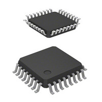
R5F21334CNFP#U0 Renesas Electronics America, R5F21334CNFP#U0 Datasheet - Page 433

R5F21334CNFP#U0
Manufacturer Part Number
R5F21334CNFP#U0
Description
MCU 1KB FLASH 16K ROM 32-LQFP
Manufacturer
Renesas Electronics America
Series
R8C/3x/33Cr
Datasheet
1.R5F21331CNFPU0.pdf
(622 pages)
Specifications of R5F21334CNFP#U0
Core Processor
R8C
Core Size
16/32-Bit
Speed
20MHz
Connectivity
I²C, LIN, SIO, SSU, UART/USART
Peripherals
POR, PWM, Voltage Detect, WDT
Number Of I /o
27
Program Memory Size
16KB (16K x 8)
Program Memory Type
FLASH
Ram Size
1.5K x 8
Voltage - Supply (vcc/vdd)
1.8 V ~ 5.5 V
Data Converters
A/D 12x10b; D/A 2x8b
Oscillator Type
Internal
Operating Temperature
-20°C ~ 85°C
Package / Case
32-LQFP
Lead Free Status / RoHS Status
Lead free / RoHS Compliant
Eeprom Size
-
Available stocks
Company
Part Number
Manufacturer
Quantity
Price
Part Number:
R5F21334CNFP#U0R5F21334CNFP#V2
Manufacturer:
Renesas Electronics America
Quantity:
10 000
- Current page: 433 of 622
- Download datasheet (7Mb)
R8C/33C Group
REJ09B0570-0100 Rev.1.00 Dec. 14, 2009
Page 403 of 589
25. I
The I
I
25.1
2
Table 25.1
Note:
C bus.
Communication formats • I
I/O pins
Transfer clocks
Receive error detection • Overrun error detection (clock synchronous serial format)
Interrupt sources
Selectable functions
Table 25.1 lists the I
Figure 25.2 shows the External Circuit Connection Example of Pins SCL and SDA, Table 25.2 lists the Pin
Configuration of I
1. All sources use one interrupt vector for I
2
2
C bus interface is the circuit that performs serial communication based on the data transfer format of the Philips
C bus Interface
Overview
Item
I
2
C bus Interface Specifications
2
C bus Interface.
2
C bus Interface Specifications, Figure 25.1 shows an I
• Clock synchronous serial format
SCL (I/O): Serial clock I/O pin
SDA (I/O): Serial data I/O pin
• When the MST bit in the ICCR1 register is set to 0.
• When the MST bit in the ICCR1 register is set to 1.
• I
• Clock synchronous serial format ...... 4 sources
• I
• Clock synchronous serial format
• SDA digital delay
2
- Selectable as master/slave device.
- Continuous transmit/receive operation (because the shift register, transmit
- Start/stop conditions are automatically generated in master mode.
- Automatic loading of the acknowledge bit during transmission
- Bit synchronization/wait function (In master mode, the state of the SCL
- Support for direct drive of pins SCL and SDA (N-channel open-drain output)
- Continuous transmit/receive operation (because the shift register, transmit
External clock (input from the SCL pin)
Internal clock selected by bits CKS0 to CKS3 in the ICCR1 register and bits
IICTCTWI and IICTCHALF in the PINSR register (output from the SCL pin)
Indicates an overrun error during reception. When the last bit of the next unit
of data is received while the RDRF bit in the ICSR register is set to 1 (data in
the ICDRR register), the AL bit is set to 1.
2
Transmit data empty (including when slave address matches), end of
transmission, receive data full (including when slave address matches),
arbitration lost, NACK detection, and stop condition detection
Transmit data empty, end of transmission, receive data full, and overrun error
2
- Selectable output level for the acknowledge signal during reception.
- MSB-first or LSB-first selectable as the data transfer direction.
- Digital delay value for the SDA pin selectable by bits SDADLY0 to
SDADLY1 in the PINSR register.
C bus format
C bus format .................................. 6 sources
C bus format
data register, and receive data register are independent.)
signal is monitored per bit and the timing is synchronized automatically. If
the transfer is not possible yet, the SCL signal goes “L” and the interface
stands by.)
data register, and receive data register are independent.)
2
C bus interface.
Specification
2
C bus interface Block Diagram, and
(1)
(1)
25. I
2
C bus Interface
Related parts for R5F21334CNFP#U0
Image
Part Number
Description
Manufacturer
Datasheet
Request
R

Part Number:
Description:
KIT STARTER FOR M16C/29
Manufacturer:
Renesas Electronics America
Datasheet:

Part Number:
Description:
KIT STARTER FOR R8C/2D
Manufacturer:
Renesas Electronics America
Datasheet:

Part Number:
Description:
R0K33062P STARTER KIT
Manufacturer:
Renesas Electronics America
Datasheet:

Part Number:
Description:
KIT STARTER FOR R8C/23 E8A
Manufacturer:
Renesas Electronics America
Datasheet:

Part Number:
Description:
KIT STARTER FOR R8C/25
Manufacturer:
Renesas Electronics America
Datasheet:

Part Number:
Description:
KIT STARTER H8S2456 SHARPE DSPLY
Manufacturer:
Renesas Electronics America
Datasheet:

Part Number:
Description:
KIT STARTER FOR R8C38C
Manufacturer:
Renesas Electronics America
Datasheet:

Part Number:
Description:
KIT STARTER FOR R8C35C
Manufacturer:
Renesas Electronics America
Datasheet:

Part Number:
Description:
KIT STARTER FOR R8CL3AC+LCD APPS
Manufacturer:
Renesas Electronics America
Datasheet:

Part Number:
Description:
KIT STARTER FOR RX610
Manufacturer:
Renesas Electronics America
Datasheet:

Part Number:
Description:
KIT STARTER FOR R32C/118
Manufacturer:
Renesas Electronics America
Datasheet:

Part Number:
Description:
KIT DEV RSK-R8C/26-29
Manufacturer:
Renesas Electronics America
Datasheet:

Part Number:
Description:
KIT STARTER FOR SH7124
Manufacturer:
Renesas Electronics America
Datasheet:

Part Number:
Description:
KIT STARTER FOR H8SX/1622
Manufacturer:
Renesas Electronics America
Datasheet:

Part Number:
Description:
KIT DEV FOR SH7203
Manufacturer:
Renesas Electronics America
Datasheet:


