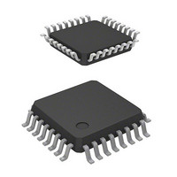
R5F21334CNFP#U0 Renesas Electronics America, R5F21334CNFP#U0 Datasheet - Page 571

R5F21334CNFP#U0
Manufacturer Part Number
R5F21334CNFP#U0
Description
MCU 1KB FLASH 16K ROM 32-LQFP
Manufacturer
Renesas Electronics America
Series
R8C/3x/33Cr
Datasheet
1.R5F21331CNFPU0.pdf
(622 pages)
Specifications of R5F21334CNFP#U0
Core Processor
R8C
Core Size
16/32-Bit
Speed
20MHz
Connectivity
I²C, LIN, SIO, SSU, UART/USART
Peripherals
POR, PWM, Voltage Detect, WDT
Number Of I /o
27
Program Memory Size
16KB (16K x 8)
Program Memory Type
FLASH
Ram Size
1.5K x 8
Voltage - Supply (vcc/vdd)
1.8 V ~ 5.5 V
Data Converters
A/D 12x10b; D/A 2x8b
Oscillator Type
Internal
Operating Temperature
-20°C ~ 85°C
Package / Case
32-LQFP
Lead Free Status / RoHS Status
Lead free / RoHS Compliant
Eeprom Size
-
Available stocks
Company
Part Number
Manufacturer
Quantity
Price
Part Number:
R5F21334CNFP#U0R5F21334CNFP#V2
Manufacturer:
Renesas Electronics America
Quantity:
10 000
- Current page: 571 of 622
- Download datasheet (7Mb)
R8C/33C Group
REJ09B0570-0100 Rev.1.00 Dec. 14, 2009
Page 541 of 589
Figure 32.3
Table 32.10
Notes:
Table 32.11
Notes:
V
−
−
−
t
t
d(E-A)
rth
det2
reset signal
Symbol
Power V
Symbol
1. The measurement condition is V
2. Time until the voltage monitor 2 interrupt request is generated after the voltage passes V
3. Necessary time until the voltage detection circuit operates after setting to 1 again after setting the VCA27 bit in the VCA2
1. The measurement condition is T
2. To use the power-on reset function, enable voltage monitor 0 reset by setting the LVDAS bit in the OFS register to 0.
Notes:
External
Internal
1. V
2. t
V
register to 0.
0.5 V
det0
Circuit for details.
a power-on reset. When turning on the power after it falls with voltage monitor 0 reset disabled, maintain
t
w(por)
w(por)
CC
det0
(1)
Voltage detection level Vdet2_0
Hysteresis width at the rising of Vcc in voltage detection
2 circuit
Voltage detection 2 circuit response time
Voltage detection circuit self power consumption
Waiting time until voltage detection circuit operation
starts
External power V
indicates the voltage detection level of the voltage detection 0 circuit. Refer to 6. Voltage Detection
indicates the duration the external power V
for 1 ms or more.
Power-on Reset Circuit
Voltage Detection 2 Circuit Electrical Characteristics
Power-on Reset Circuit Electrical Characteristics
(3)
t
w(por)
(2)
CC
Parameter
rise gradient
t
Parameter
rth
opr
CC
= 1.8 V to 5.5 V and T
= − 20 to 85 ° C (N version) / − 40 to 85 ° C (D version), unless otherwise specified.
(2)
f
OCO-S
1
(2)
circuit response time
Voltage detection 0
× 32
CC
opr
(1)
must be held below the valid voltage (0.5 V) to enable
= − 20 to 85 ° C (N version) / − 40 to 85 ° C (D version).
At the falling of V
At the falling of Vcc from
5 V to (Vdet2_0 − 0.1) V
VCA27 = 1, V
Condition
Condition
CC
= 5.0 V
CC
t
rth
Min.
0
det2
3.70
Min.
32. Electrical Characteristics
.
−
−
−
−
Standard
Typ.
f
OCO-S
Standard
−
1
Typ.
4.00
0.10
1.7
20
−
50,000 mV/msec
× 32
Max.
V
Max.
4.30
150
100
det0
−
−
(1)
Unit
Unit
µ A
µ s
µ s
V
V
Related parts for R5F21334CNFP#U0
Image
Part Number
Description
Manufacturer
Datasheet
Request
R

Part Number:
Description:
KIT STARTER FOR M16C/29
Manufacturer:
Renesas Electronics America
Datasheet:

Part Number:
Description:
KIT STARTER FOR R8C/2D
Manufacturer:
Renesas Electronics America
Datasheet:

Part Number:
Description:
R0K33062P STARTER KIT
Manufacturer:
Renesas Electronics America
Datasheet:

Part Number:
Description:
KIT STARTER FOR R8C/23 E8A
Manufacturer:
Renesas Electronics America
Datasheet:

Part Number:
Description:
KIT STARTER FOR R8C/25
Manufacturer:
Renesas Electronics America
Datasheet:

Part Number:
Description:
KIT STARTER H8S2456 SHARPE DSPLY
Manufacturer:
Renesas Electronics America
Datasheet:

Part Number:
Description:
KIT STARTER FOR R8C38C
Manufacturer:
Renesas Electronics America
Datasheet:

Part Number:
Description:
KIT STARTER FOR R8C35C
Manufacturer:
Renesas Electronics America
Datasheet:

Part Number:
Description:
KIT STARTER FOR R8CL3AC+LCD APPS
Manufacturer:
Renesas Electronics America
Datasheet:

Part Number:
Description:
KIT STARTER FOR RX610
Manufacturer:
Renesas Electronics America
Datasheet:

Part Number:
Description:
KIT STARTER FOR R32C/118
Manufacturer:
Renesas Electronics America
Datasheet:

Part Number:
Description:
KIT DEV RSK-R8C/26-29
Manufacturer:
Renesas Electronics America
Datasheet:

Part Number:
Description:
KIT STARTER FOR SH7124
Manufacturer:
Renesas Electronics America
Datasheet:

Part Number:
Description:
KIT STARTER FOR H8SX/1622
Manufacturer:
Renesas Electronics America
Datasheet:

Part Number:
Description:
KIT DEV FOR SH7203
Manufacturer:
Renesas Electronics America
Datasheet:


