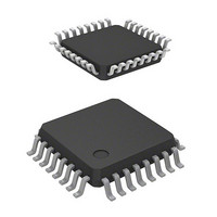
R5F21334CNFP#U0 Renesas Electronics America, R5F21334CNFP#U0 Datasheet - Page 607

R5F21334CNFP#U0
Manufacturer Part Number
R5F21334CNFP#U0
Description
MCU 1KB FLASH 16K ROM 32-LQFP
Manufacturer
Renesas Electronics America
Series
R8C/3x/33Cr
Datasheet
1.R5F21331CNFPU0.pdf
(622 pages)
Specifications of R5F21334CNFP#U0
Core Processor
R8C
Core Size
16/32-Bit
Speed
20MHz
Connectivity
I²C, LIN, SIO, SSU, UART/USART
Peripherals
POR, PWM, Voltage Detect, WDT
Number Of I /o
27
Program Memory Size
16KB (16K x 8)
Program Memory Type
FLASH
Ram Size
1.5K x 8
Voltage - Supply (vcc/vdd)
1.8 V ~ 5.5 V
Data Converters
A/D 12x10b; D/A 2x8b
Oscillator Type
Internal
Operating Temperature
-20°C ~ 85°C
Package / Case
32-LQFP
Lead Free Status / RoHS Status
Lead free / RoHS Compliant
Eeprom Size
-
Available stocks
Company
Part Number
Manufacturer
Quantity
Price
Part Number:
R5F21334CNFP#U0R5F21334CNFP#V2
Manufacturer:
Renesas Electronics America
Quantity:
10 000
- Current page: 607 of 622
- Download datasheet (7Mb)
R8C/33C Group
REJ09B0570-0100 Rev.1.00 Dec. 14, 2009
Page 577 of 589
33.12 Notes on Synchronous Serial Communication Unit
33.13 Notes on I
33.14 Notes on Hardware LIN
33.15 Notes on A/D Converter
33.11.2 Special Mode 1 (I
Set the IICSEL bit in the SSUIICSR register to 0 (select SSU function) to use the synchronous serial
communication unit function.
For the time-out processing of the header and response fields, use another timer to measure the duration of time
with a Synch Break detection interrupt as the starting point.
•
•
•
•
•
•
•
•
Write to the ADMOD register, the ADINSEL register, the ADCON0 register (other than ADST bit), the
ADCON1 register, the OCVREFCR register when A/D conversion is stopped (before a trigger occurs).
To use the A/D converter in repeat mode 0, repeat mode 1, or repeat sweep mode, select the frequency of the A/D
converter operating clock φAD or more for the CPU clock during A/D conversion.
Do not select fOCO-F as φAD.
Connect 0.1 µF capacitor between the VREF pin and AVSS pin.
Do not enter stop mode during A/D conversion.
Do not enter wait mode during A/D conversion regardless of the state of the CM02 bit in the CM0 register (1:
Peripheral function clock stops in wait mode or 0: Peripheral function clock does not stop in wait mode).
Do not set the FMSTP bit in the FMR0 register to 1 (flash memory stops) or the FMR27 bit to 1 (low-current-
consumption read mode enabled) during A/D conversion. Otherwise, the A/D conversion result will be
undefined.
Do not change the CKS2 bit in the ADMOD register while fOCO-F is stopped.
During an A/D conversion operation, if the ADST bit in the ADCON0 register is set to 0 (A/D conversion stops)
by a program to forcibly terminate A/D conversion, the conversion result of the A/D converter is undefined and
no interrupt is generated. The value of the ADi register before A/D conversion may also be undefined.
If the ADST bit is set to 0 by a program, do not use the value of all the ADi register.
When generating start, stop, and restart conditions, set the STSPSEL bit in the U2SMR4 register to 0 and wait
for more than half cycle of the transfer clock before changing each condition generation bit (STAREQ,
RSTAREQ, and STPREQ) from 0 to 1.
To use the I
selected).
2
C bus interface, set the IICSEL bit in the SSUIICSR register to 1 (I
2
C bus Interface
2
C Mode)
2
C bus interface function
33. Usage Notes
Related parts for R5F21334CNFP#U0
Image
Part Number
Description
Manufacturer
Datasheet
Request
R

Part Number:
Description:
KIT STARTER FOR M16C/29
Manufacturer:
Renesas Electronics America
Datasheet:

Part Number:
Description:
KIT STARTER FOR R8C/2D
Manufacturer:
Renesas Electronics America
Datasheet:

Part Number:
Description:
R0K33062P STARTER KIT
Manufacturer:
Renesas Electronics America
Datasheet:

Part Number:
Description:
KIT STARTER FOR R8C/23 E8A
Manufacturer:
Renesas Electronics America
Datasheet:

Part Number:
Description:
KIT STARTER FOR R8C/25
Manufacturer:
Renesas Electronics America
Datasheet:

Part Number:
Description:
KIT STARTER H8S2456 SHARPE DSPLY
Manufacturer:
Renesas Electronics America
Datasheet:

Part Number:
Description:
KIT STARTER FOR R8C38C
Manufacturer:
Renesas Electronics America
Datasheet:

Part Number:
Description:
KIT STARTER FOR R8C35C
Manufacturer:
Renesas Electronics America
Datasheet:

Part Number:
Description:
KIT STARTER FOR R8CL3AC+LCD APPS
Manufacturer:
Renesas Electronics America
Datasheet:

Part Number:
Description:
KIT STARTER FOR RX610
Manufacturer:
Renesas Electronics America
Datasheet:

Part Number:
Description:
KIT STARTER FOR R32C/118
Manufacturer:
Renesas Electronics America
Datasheet:

Part Number:
Description:
KIT DEV RSK-R8C/26-29
Manufacturer:
Renesas Electronics America
Datasheet:

Part Number:
Description:
KIT STARTER FOR SH7124
Manufacturer:
Renesas Electronics America
Datasheet:

Part Number:
Description:
KIT STARTER FOR H8SX/1622
Manufacturer:
Renesas Electronics America
Datasheet:

Part Number:
Description:
KIT DEV FOR SH7203
Manufacturer:
Renesas Electronics America
Datasheet:


