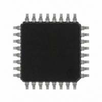
R5F21272SNFP#U0 Renesas Electronics America, R5F21272SNFP#U0 Datasheet - Page 365

R5F21272SNFP#U0
Manufacturer Part Number
R5F21272SNFP#U0
Description
IC R8C/27 MCU FLASH 32LQFP
Manufacturer
Renesas Electronics America
Series
R8C/2x/27r
Datasheet
1.R5F21272SDFPU0.pdf
(487 pages)
Specifications of R5F21272SNFP#U0
Core Processor
R8C
Core Size
16/32-Bit
Speed
20MHz
Connectivity
I²C, LIN, SIO, SSU, UART/USART
Peripherals
LED, POR, Voltage Detect, WDT
Number Of I /o
25
Program Memory Size
8KB (8K x 8)
Program Memory Type
FLASH
Ram Size
512 x 8
Voltage - Supply (vcc/vdd)
2.2 V ~ 5.5 V
Data Converters
A/D 12x10b
Oscillator Type
Internal
Operating Temperature
-20°C ~ 85°C
Package / Case
32-LQFP
For Use With
R0K521276S000BE - KIT DEV RSK-R8C/26-29R0E521000EPB00 - PROBE EMULATOR FOR PC7501
Lead Free Status / RoHS Status
Lead free / RoHS Compliant
Eeprom Size
-
Available stocks
Company
Part Number
Manufacturer
Quantity
Price
Part Number:
R5F21272SNFP#U0R5F21272SNFP#V2
Manufacturer:
Renesas Electronics America
Quantity:
10 000
- Current page: 365 of 487
- Download datasheet (5Mb)
R8C/26 Group, R8C/27 Group
Rev.2.10
REJ09B0278-0210
Figure 18.6
A/D Control Register 0
b7 b6 b5 b4
NOTES:
1.
2.
3.
4.
0
If the ADCON0 register is rew ritten during A/D conversion, the conversion result is undefined.
After changing A/D operation mode, select the analog input pin again.
Set øAD frequency to 10 MHz or below .
The analog input pin can be selected according to a combination of bits CH0 to CH2 and the ADGSEL0 bit.
Sep 26, 2008
CH2 to CH0
b3 b2 b1 b0
1
000b
001b
010b
011b
100b
101b
110b
111b
ADCON0 Register in Repeat Mode
ADGSEL0 = 0
Bit Symbol
ADGSEL0
ADCON0
(1)
Symbol
ADST
CKS0
CH0
CH1
CH2
(b5)
AN0
AN1
AN2
AN3
AN4
AN5
AN6
AN7
MD
Page 346 of 453
—
Analog input pin select bits (Note 4)
A/D operating mode select
bit
A/D input group select bit
Reserved bit
A/D conversion start flag
Frequency select bit 0
(2)
ADGSEL0 = 1
Do not set.
Address
Bit Name
00D6h
AN10
AN11
AN8
AN9
(4)
1 : Repeat mode
0 : Selects port P0 group (AN0 to AN7)
1 : Selects port P1 group (AN8 to AN11)
Set to 0.
0 : Stops A/D conversion
1 : Starts A/D conversion
[When CKS1 in ADCON1 register = 0]
0 : Select f4
1 : Select f2
[When CKS1 in ADCON1 register = 1]
0 : Select f1
1 : Do not set.
(3)
After Reset
Function
00h
18. A/D Converter
RW
RW
RW
RW
RW
RW
RW
RW
RW
Related parts for R5F21272SNFP#U0
Image
Part Number
Description
Manufacturer
Datasheet
Request
R

Part Number:
Description:
KIT STARTER FOR M16C/29
Manufacturer:
Renesas Electronics America
Datasheet:

Part Number:
Description:
KIT STARTER FOR R8C/2D
Manufacturer:
Renesas Electronics America
Datasheet:

Part Number:
Description:
R0K33062P STARTER KIT
Manufacturer:
Renesas Electronics America
Datasheet:

Part Number:
Description:
KIT STARTER FOR R8C/23 E8A
Manufacturer:
Renesas Electronics America
Datasheet:

Part Number:
Description:
KIT STARTER FOR R8C/25
Manufacturer:
Renesas Electronics America
Datasheet:

Part Number:
Description:
KIT STARTER H8S2456 SHARPE DSPLY
Manufacturer:
Renesas Electronics America
Datasheet:

Part Number:
Description:
KIT STARTER FOR R8C38C
Manufacturer:
Renesas Electronics America
Datasheet:

Part Number:
Description:
KIT STARTER FOR R8C35C
Manufacturer:
Renesas Electronics America
Datasheet:

Part Number:
Description:
KIT STARTER FOR R8CL3AC+LCD APPS
Manufacturer:
Renesas Electronics America
Datasheet:

Part Number:
Description:
KIT STARTER FOR RX610
Manufacturer:
Renesas Electronics America
Datasheet:

Part Number:
Description:
KIT STARTER FOR R32C/118
Manufacturer:
Renesas Electronics America
Datasheet:

Part Number:
Description:
KIT DEV RSK-R8C/26-29
Manufacturer:
Renesas Electronics America
Datasheet:

Part Number:
Description:
KIT STARTER FOR SH7124
Manufacturer:
Renesas Electronics America
Datasheet:

Part Number:
Description:
KIT STARTER FOR H8SX/1622
Manufacturer:
Renesas Electronics America
Datasheet:

Part Number:
Description:
KIT DEV FOR SH7203
Manufacturer:
Renesas Electronics America
Datasheet:


