R5F21274SNFP#U0 Renesas Electronics America, R5F21274SNFP#U0 Datasheet - Page 360
R5F21274SNFP#U0
Manufacturer Part Number
R5F21274SNFP#U0
Description
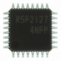
IC R8C/27 MCU FLASH 32LQFP
Manufacturer
Renesas Electronics America
Series
R8C/2x/27r
Datasheet
1.R5F21272SDFPU0.pdf
(487 pages)
Specifications of R5F21274SNFP#U0
Core Processor
R8C
Core Size
16/32-Bit
Speed
20MHz
Connectivity
I²C, LIN, SIO, SSU, UART/USART
Peripherals
LED, POR, Voltage Detect, WDT
Number Of I /o
25
Program Memory Size
16KB (16K x 8)
Program Memory Type
FLASH
Ram Size
1K x 8
Voltage - Supply (vcc/vdd)
2.2 V ~ 5.5 V
Data Converters
A/D 12x10b
Oscillator Type
Internal
Operating Temperature
-20°C ~ 85°C
Package / Case
32-LQFP
For Use With
R0K521276S000BE - KIT DEV RSK-R8C/26-29R0E521000EPB00 - PROBE EMULATOR FOR PC7501
Lead Free Status / RoHS Status
Lead free / RoHS Compliant
Eeprom Size
-
Available stocks
Company
Part Number
Manufacturer
Quantity
Price

Part Number:
R5F21274SNFP#U0R5F21274SNFP#V2
Manufacturer:
Renesas Electronics America
Quantity:
10 000


R8C/26 Group, R8C/27 Group
Rev.2.10
REJ09B0278-0210
Figure 18.3
A/D Control Register 1
A/D Control Register 2
A/D Register
(b15)
b7 b6 b5 b4
NOTES:
b7 b6 b5 b4
NOTE:
b7
0 0
1.
2.
3. When the VCUT bit is set to 1 (connected) from 0 (not connected), w ait for 1 µs or more before starting
1.
If the ADCON1 register is rew ritten during A/D conversion, the conversion result is undefined.
Set the BITS bit to 0 (8-bit mode) in repeat mode.
A/D conversion.
If the ADCON2 register is rew ritten during A/D conversion, the conversion result is undefined.
Sep 26, 2008
b3 b2
b3 b2 b1 b0
0
0 0
0 0
Registers ADCON1, ADCON2, and AD
b1 b0
(b8)
b0
0
b7
8 low -order bits in A/D conversion result
2 high-order bits in A/D conversion result
Nothing is assigned. If necessary, set to 0.
When read, the content is 0.
Bit Symbol
Bit Symbol
ADCON1
ADCON2
(b2-b0)
(b6-b7)
(b3-b1)
(b7-b4)
Symbol
Symbol
(1)
(1)
CKS1
VCUT
BITS
SMP
When BITS bit in ADCON1 register is
Page 341 of 453
—
—
—
—
set to 1 (10-bit mode).
Reserved bits
8/10-bit mode select bit
Frequency select bit 1
VREF connect bit
Reserved bits
A/D conversion method select bit
Reserved bits
Nothing is assigned. If necessary, set to 0.
When read, the content is 0.
b0
Address
Bit Name
00D7h
Address
Bit Name
00D4h
(3)
Symbol
(2)
AD
Set to 0.
0 : 8-bit mode
1 : 10-bit mode
Refer to the description of the CKS0 bit in the
ADCON0 register function.
0 : VREF not connected
1 : VREF connected
Set to 0.
Function
A/D conversion result
When read, the content is undefined.
0 : Without sample and hold
1 : With sample and hold
Set to 0.
00C1h-00C0h
When BITS bit in ADCON1 register is
Address
set to 0 (8-bit mode).
After Reset
Function
00h
After Reset
Function
00h
After Reset
Undefined
18. A/D Converter
RW
RW
RW
RW
RW
RW
RW
RW
RW
RW
—
RO
RO
—
Related parts for R5F21274SNFP#U0
Image
Part Number
Description
Manufacturer
Datasheet
Request
R

Part Number:
Description:
KIT STARTER FOR M16C/29
Manufacturer:
Renesas Electronics America
Datasheet:

Part Number:
Description:
KIT STARTER FOR R8C/2D
Manufacturer:
Renesas Electronics America
Datasheet:

Part Number:
Description:
R0K33062P STARTER KIT
Manufacturer:
Renesas Electronics America
Datasheet:

Part Number:
Description:
KIT STARTER FOR R8C/23 E8A
Manufacturer:
Renesas Electronics America
Datasheet:

Part Number:
Description:
KIT STARTER FOR R8C/25
Manufacturer:
Renesas Electronics America
Datasheet:

Part Number:
Description:
KIT STARTER H8S2456 SHARPE DSPLY
Manufacturer:
Renesas Electronics America
Datasheet:

Part Number:
Description:
KIT STARTER FOR R8C38C
Manufacturer:
Renesas Electronics America
Datasheet:

Part Number:
Description:
KIT STARTER FOR R8C35C
Manufacturer:
Renesas Electronics America
Datasheet:

Part Number:
Description:
KIT STARTER FOR R8CL3AC+LCD APPS
Manufacturer:
Renesas Electronics America
Datasheet:
Part Number:
Description:
KIT STARTER FOR RX610
Manufacturer:
Renesas Electronics America
Datasheet:

Part Number:
Description:
KIT STARTER FOR R32C/118
Manufacturer:
Renesas Electronics America
Datasheet:

Part Number:
Description:
KIT DEV RSK-R8C/26-29
Manufacturer:
Renesas Electronics America
Datasheet:

Part Number:
Description:
KIT STARTER FOR SH7124
Manufacturer:
Renesas Electronics America
Datasheet:

Part Number:
Description:
KIT STARTER FOR H8SX/1622
Manufacturer:
Renesas Electronics America
Datasheet:

Part Number:
Description:
KIT DEV FOR SH7203
Manufacturer:
Renesas Electronics America
Datasheet: