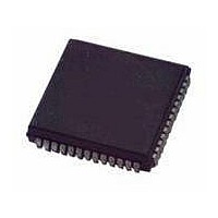
MC68HC11E0CFNE2R Freescale Semiconductor, MC68HC11E0CFNE2R Datasheet - Page 53

MC68HC11E0CFNE2R
Manufacturer Part Number
MC68HC11E0CFNE2R
Description
IC MCU 8BIT 2MHZ 52-PLCC
Manufacturer
Freescale Semiconductor
Series
HC11r
Datasheet
1.MC68HC11E0CFNE2R.pdf
(242 pages)
Specifications of MC68HC11E0CFNE2R
Core Processor
HC11
Core Size
8-Bit
Speed
2MHz
Connectivity
SCI, SPI
Peripherals
POR, WDT
Number Of I /o
38
Program Memory Type
ROMless
Ram Size
512 x 8
Voltage - Supply (vcc/vdd)
4.5 V ~ 5.5 V
Data Converters
A/D 8x8b
Oscillator Type
Internal
Operating Temperature
-40°C ~ 85°C
Package / Case
52-PLCC
Processor Series
HC11E
Core
HC11
Data Bus Width
8 bit
Data Ram Size
512 B
Interface Type
SCI, SPI
Maximum Clock Frequency
2 MHz
Number Of Programmable I/os
38
Number Of Timers
8
Maximum Operating Temperature
+ 85 C
Mounting Style
SMD/SMT
Minimum Operating Temperature
- 40 C
On-chip Adc
8 bit, 8 Channel
Lead Free Status / RoHS Status
Lead free / RoHS Compliant
Eeprom Size
-
Program Memory Size
-
Lead Free Status / Rohs Status
Details
Available stocks
Company
Part Number
Manufacturer
Quantity
Price
Company:
Part Number:
MC68HC11E0CFNE2R
Manufacturer:
Freescale Semiconductor
Quantity:
10 000
- Current page: 53 of 242
- Download datasheet (2Mb)
2.5.1.2 EPROM and EEPROM Programming Control Register
The EPROM and EEPROM programming control register (PPROG) selects and controls the EEPROM
programming function. Bits in PPROG enable the programming voltage, control the latching of data to be
programmed, and select the method of erasure (for example, byte, row, etc.).
ODD — Program Odd Rows in Half of EEPROM (Test) Bit
EVEN — Program Even Rows in Half of EEPROM (Test) Bit
ELAT — EPROM/OTPROM Latch Control Bit
BYTE — Byte/Other EEPROM Erase Mode Bit
ROW — Row/All EEPROM Erase Mode Bit
ERASE — Erase Mode Select Bit
EELAT — EEPROM Latch Control Bit
Freescale Semiconductor
For the MC68HC711E9, EPGM enables the high voltage necessary for both EPROM/OTPROM and
EEPROM programming.
For MC68HC711E9, ELAT and EELAT are mutually exclusive and cannot both equal 1.
This bit overrides the ROW bit.
If BYTE is 1, ROW has no meaning.
0 = EPROM address and data bus configured for normal reads
1 = EPROM address and data bus configured for programming
0 = Row or bulk erase
1 = Erase only one byte
0 = Bulk erase
1 = Row erase
0 = Normal read or program mode
1 = Erase mode
0 = EEPROM address and data bus configured for normal reads and cannot be programmed
1 = EEPROM address and data bus configured for programming or erasing and cannot be read
1. MC68HC711E9 only
Address: $103B
Reset:
Read:
Write:
ODD
Bit 7
0
Figure 2-17. EPROM and EEPROM Programming
BYTE
0
0
1
1
EVEN
6
0
M68HC11E Family Data Sheet, Rev. 5.1
Control Register (PPROG)
Table 2-8. EEPROM Erase
ROW
ELAT
0
1
0
1
5
0
(1)
BYTE
Bulk erase (entire array)
Row erase (16 bytes)
Byte erase
Byte erase
4
0
ROW
3
0
Action
ERASE
2
0
EELAT
0
1
EPGM
Bit 0
0
EEPROM
53
Related parts for MC68HC11E0CFNE2R
Image
Part Number
Description
Manufacturer
Datasheet
Request
R
Part Number:
Description:
Manufacturer:
Freescale Semiconductor, Inc
Datasheet:
Part Number:
Description:
Manufacturer:
Freescale Semiconductor, Inc
Datasheet:
Part Number:
Description:
Manufacturer:
Freescale Semiconductor, Inc
Datasheet:
Part Number:
Description:
Manufacturer:
Freescale Semiconductor, Inc
Datasheet:
Part Number:
Description:
Manufacturer:
Freescale Semiconductor, Inc
Datasheet:
Part Number:
Description:
Manufacturer:
Freescale Semiconductor, Inc
Datasheet:
Part Number:
Description:
Manufacturer:
Freescale Semiconductor, Inc
Datasheet:
Part Number:
Description:
Manufacturer:
Freescale Semiconductor, Inc
Datasheet:
Part Number:
Description:
Manufacturer:
Freescale Semiconductor, Inc
Datasheet:
Part Number:
Description:
Manufacturer:
Freescale Semiconductor, Inc
Datasheet:
Part Number:
Description:
Manufacturer:
Freescale Semiconductor, Inc
Datasheet:
Part Number:
Description:
Manufacturer:
Freescale Semiconductor, Inc
Datasheet:
Part Number:
Description:
Manufacturer:
Freescale Semiconductor, Inc
Datasheet:
Part Number:
Description:
Manufacturer:
Freescale Semiconductor, Inc
Datasheet:
Part Number:
Description:
Manufacturer:
Freescale Semiconductor, Inc
Datasheet:


