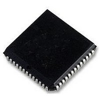
MC68HC11E1CFNE2R Freescale Semiconductor, MC68HC11E1CFNE2R Datasheet - Page 137

MC68HC11E1CFNE2R
Manufacturer Part Number
MC68HC11E1CFNE2R
Description
IC MCU 8BIT 2MHZ 52-PLCC
Manufacturer
Freescale Semiconductor
Series
HC11r
Specifications of MC68HC11E1CFNE2R
Core Processor
HC11
Core Size
8-Bit
Speed
3MHz
Connectivity
SCI, SPI
Peripherals
POR, WDT
Number Of I /o
38
Program Memory Type
ROMless
Eeprom Size
512 x 8
Ram Size
512 x 8
Voltage - Supply (vcc/vdd)
4.5 V ~ 5.5 V
Data Converters
A/D 8x8b
Oscillator Type
Internal
Operating Temperature
-40°C ~ 85°C
Package / Case
52-PLCC
Controller Family/series
68HC11
No. Of I/o's
38
Eeprom Memory Size
512Byte
Ram Memory Size
512Byte
Cpu Speed
2MHz
No. Of Timers
1
Embedded Interface Type
SCI, SPI
Rohs Compliant
Yes
Processor Series
HC11E
Core
HC11
Data Bus Width
8 bit
Data Ram Size
512 B
Interface Type
SCI, SPI
Maximum Clock Frequency
2 MHz
Number Of Programmable I/os
38
Number Of Timers
8
Maximum Operating Temperature
+ 85 C
Mounting Style
SMD/SMT
Minimum Operating Temperature
- 40 C
On-chip Adc
8 bit, 8 Channel
Lead Free Status / RoHS Status
Lead free / RoHS Compliant
Program Memory Size
-
Lead Free Status / Rohs Status
Details
Available stocks
Company
Part Number
Manufacturer
Quantity
Price
Company:
Part Number:
MC68HC11E1CFNE2R
Manufacturer:
Freescale Semiconductor
Quantity:
10 000
Company:
Part Number:
MC68HC11E1CFNE2R2
Manufacturer:
FREESCALE
Quantity:
5 510
Company:
Part Number:
MC68HC11E1CFNE2R2
Manufacturer:
MICROCHIP
Quantity:
5 510
- Current page: 137 of 242
- Download datasheet (2Mb)
9.4.5 Timer Counter Register
The 16-bit read-only TCNT register contains the prescaled value of the 16-bit timer. A full counter read
addresses the most significant byte (MSB) first. A read of this address causes the least significant byte
(LSB) to be latched into a buffer for the next CPU cycle so that a double-byte read returns the full 16-bit
state of the counter at the time of the MSB read cycle.
9.4.6 Timer Control Register 1
The bits of this register specify the action taken as a result of a successful OCx compare.
OM[2:5] — Output Mode Bits
OL[2:5] — Output Level Bits
Freescale Semiconductor
These control bit pairs are encoded to specify the action taken after a successful OCx compare. OC5
functions only if the I4/O5 bit in the PACTL register is clear. Refer to
Register name: Timer Counter Register (High)
Register name: Timer Counter Register (Low)
Address:
Reset:
Reset:
Reset:
Read:
Read:
Read:
Write:
Write:
Write:
$1020
Bit 15
OM2
Bit 7
Bit 7
Bit 7
Bit 7
OMx
0
0
0
0
0
1
1
Figure 9-16. Timer Control Register 1 (TCTL1)
Figure 9-15. Timer Counter Register (TCNT)
Table 9-3. Timer Output Compare Actions
= Unimplemented
OLx
Bit 14
Bit 6
OL2
0
1
0
1
0
0
6
6
6
0
M68HC11E Family Data Sheet, Rev. 5.1
Timer disconnected from output pin logic
Toggle OCx output line
Clear OCx output line to 0
Set OCx output line to 1
Bit 13
OM3
Bit 5
5
0
5
0
5
0
Action Taken on Successful Compare
Address: $100F
Address: $100E
Bit 12
Bit 4
OL3
4
0
4
0
4
0
Bit 11
OM4
Bit 3
3
0
3
0
3
0
Bit 10
Bit 2
OL4
2
0
2
0
2
0
Table 9-3
OM5
Bit 9
Bit 1
1
0
1
0
1
0
for the coding.
Bit 0
Bit 8
Bit 0
Bit 0
Bit 0
OL5
0
0
0
Output Compare
137
Related parts for MC68HC11E1CFNE2R
Image
Part Number
Description
Manufacturer
Datasheet
Request
R
Part Number:
Description:
Manufacturer:
Freescale Semiconductor, Inc
Datasheet:
Part Number:
Description:
Manufacturer:
Freescale Semiconductor, Inc
Datasheet:
Part Number:
Description:
Manufacturer:
Freescale Semiconductor, Inc
Datasheet:
Part Number:
Description:
Manufacturer:
Freescale Semiconductor, Inc
Datasheet:
Part Number:
Description:
Manufacturer:
Freescale Semiconductor, Inc
Datasheet:
Part Number:
Description:
Manufacturer:
Freescale Semiconductor, Inc
Datasheet:
Part Number:
Description:
Manufacturer:
Freescale Semiconductor, Inc
Datasheet:
Part Number:
Description:
Manufacturer:
Freescale Semiconductor, Inc
Datasheet:
Part Number:
Description:
Manufacturer:
Freescale Semiconductor, Inc
Datasheet:
Part Number:
Description:
Manufacturer:
Freescale Semiconductor, Inc
Datasheet:
Part Number:
Description:
Manufacturer:
Freescale Semiconductor, Inc
Datasheet:
Part Number:
Description:
Manufacturer:
Freescale Semiconductor, Inc
Datasheet:
Part Number:
Description:
Manufacturer:
Freescale Semiconductor, Inc
Datasheet:
Part Number:
Description:
Manufacturer:
Freescale Semiconductor, Inc
Datasheet:
Part Number:
Description:
Manufacturer:
Freescale Semiconductor, Inc
Datasheet:


