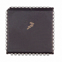
MC68HC711D3CFNE3 Freescale Semiconductor, MC68HC711D3CFNE3 Datasheet - Page 40

MC68HC711D3CFNE3
Manufacturer Part Number
MC68HC711D3CFNE3
Description
IC MCU 8BIT 2MHZ 44-PLCC
Manufacturer
Freescale Semiconductor
Series
HC11r
Specifications of MC68HC711D3CFNE3
Core Processor
HC11
Core Size
8-Bit
Speed
3MHz
Connectivity
SCI, SPI
Peripherals
POR, WDT
Number Of I /o
26
Program Memory Size
4KB (4K x 8)
Program Memory Type
OTP
Ram Size
192 x 8
Voltage - Supply (vcc/vdd)
4.5 V ~ 5.5 V
Oscillator Type
Internal
Operating Temperature
-40°C ~ 85°C
Package / Case
44-PLCC
Lead Free Status / RoHS Status
Lead free / RoHS Compliant
Eeprom Size
-
Data Converters
-
Available stocks
Company
Part Number
Manufacturer
Quantity
Price
Company:
Part Number:
MC68HC711D3CFNE3
Manufacturer:
SGS
Quantity:
6 218
Company:
Part Number:
MC68HC711D3CFNE3
Manufacturer:
Freescale Semiconductor
Quantity:
10 000
4.2.1 Priority and Mode Select Register
4-6
In the second method, the MODB/V
backup or from a second power supply, as shown in Figure 4-3. Using the MODB/
V
amount of external circuitry is operating from V
contents, reset must be held low whenever V
to SECTION 5 RESETS AND INTERRUPTS.
The four operating modes are selected with the logic states of the mode A (MODA)
and mode B (MODB) pins during reset. The MODA and MODB logic levels determine
the logic state of the special mode (SMOD) and mode A (MDA) control bits in the
HPRIO register.
After reset is released, the mode select pins no longer influence the MCU operating
mode. For single-chip mode, the MODA pin is connected to a logic zero. For expanded
mode, MODA is normally connected to V
MODA pin also functions as the load instruction register (LIR) pin when the MCU is not
in reset. The open drain active low LIR output pin drives low during the first E cycle of
each instruction. The MODB pin also functions as standby power input, V
maintains RAM contents in the absence of V
about hardware mode selection.
STBY
MODB
1
1
0
0
pin may require external hardware, but can be justified when a significant
4.8 V
NiCd
Figure 4-3 RAM Standby MODB/V
Inputs
V
DD
+
Table 4-2 Hardware Mode Select Summary
Freescale Semiconductor, Inc.
OPERATING MODES AND ON-CHIP MEMORY
MODA
V
V
For More Information On This Product,
DD
BATT
0
1
0
1
MAX
690
V
OUT
Go to: www.freescale.com
Expanded Multiplexed
Special Bootstrap
4.7k
STBY
Special Test
Single-Chip
Mode
DD
pin can supply RAM power from a battery
DD
through a pull-up resistor of 4.7 k
TO MODB/V
OF M68HC11
DD
DD
is below normal operating level. Refer
. Refer to Table 4-2 for information
STBY
. If V
RBOOT
STBY
STBY
Connections
0
0
1
0
is used to maintain RAM
Latched at Reset
SMOD
MODB/VSTBY CONN
0
0
1
1
TECHNICAL DATA
MDA
0
1
0
1
STBY,
which
The


