MC68HC705C9ACFBE Freescale Semiconductor, MC68HC705C9ACFBE Datasheet - Page 114
MC68HC705C9ACFBE
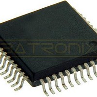
Manufacturer Part Number
MC68HC705C9ACFBE
Description
IC MCU 8BIT 44-QFP
Manufacturer
Freescale Semiconductor
Series
HC05r
Datasheet
1.MC705C9ACPE.pdf
(118 pages)
Specifications of MC68HC705C9ACFBE
Core Processor
HC05
Core Size
8-Bit
Speed
2.1MHz
Connectivity
SCI, SPI
Peripherals
POR, WDT
Number Of I /o
24
Program Memory Size
16KB (16K x 8)
Program Memory Type
OTP
Ram Size
352 x 8
Voltage - Supply (vcc/vdd)
3 V ~ 5.5 V
Oscillator Type
Internal
Operating Temperature
-40°C ~ 85°C
Package / Case
44-QFP
Processor Series
HC705C
Core
HC05
Data Bus Width
8 bit
Data Ram Size
352 B
Interface Type
SCI, SPI
Maximum Clock Frequency
2.1 MHz
Number Of Programmable I/os
31
Number Of Timers
1
Maximum Operating Temperature
+ 85 C
Mounting Style
SMD/SMT
Minimum Operating Temperature
- 40 C
On-chip Adc
8 bit
Package
44PQFP
Family Name
HC05
Maximum Speed
2.1 MHz
Operating Supply Voltage
3.3|5 V
Lead Free Status / RoHS Status
Lead free / RoHS Compliant
Eeprom Size
-
Data Converters
-
Lead Free Status / Rohs Status
Details
Available stocks
Company
Part Number
Manufacturer
Quantity
Price
Company:

Part Number:
MC68HC705C9ACFBE
Manufacturer:
FREESCALE
Quantity:
1 827
Company:
Part Number:
MC68HC705C9ACFBE
Manufacturer:
Freescale Semiconductor
Quantity:
10 000


EPROM Programming
A.4 Programming Register (PROG)
This register is used to program the EPROM array. To program a byte of EPROM, set LATCH, write data
to the desired address, and set EPGM for t
LATCH — EPROM Latch Control Bit
EPGM — EPROM Program Control Bit
114
This read/write bit controls the latching of the address and data buses when programming the EPROM.
This read/write bit controls whether the programming voltage is applied to the EPROM array. For
programming, this bit can be set only if the LATCH bit has been set previously. Both EPGM and LATCH
cannot be set in the single write.
1 = Address and data buses latched when the following instruction is a write to 1 of the EPROM
0 = EPROM address and data bus configured for normal reading
1 = Programming voltage applied to EPROM array
0 = Programming voltage not applied to EPROM array
locations. Normal reading is disabled if LATCH = 1.
Bits 7–3 and bit 1 MUST be set to 0 when writing to the EPROM
programming register.
$001X
Reset:
Read:
Write:
Bit 7
0
MC68HC05C9A Advance Information Data Sheet, Rev. 4.1
Figure A-1. EPROM Programming Register
6
0
5
0
EPGM
.
NOTE
4
0
3
0
LATCH
2
0
1
0
Freescale Semiconductor
EPGM
Bit 0
0
Related parts for MC68HC705C9ACFBE
Image
Part Number
Description
Manufacturer
Datasheet
Request
R

Part Number:
Description:
APPENDIX A ELECTRICAL CHARACTERISTICS
Manufacturer:
FREESCALE [Freescale Semiconductor, Inc]
Datasheet:

Part Number:
Description:
Manufacturer:
Freescale Semiconductor, Inc
Datasheet:
Part Number:
Description:
Manufacturer:
Freescale Semiconductor, Inc
Datasheet:
Part Number:
Description:
Manufacturer:
Freescale Semiconductor, Inc
Datasheet:
Part Number:
Description:
Manufacturer:
Freescale Semiconductor, Inc
Datasheet:
Part Number:
Description:
Manufacturer:
Freescale Semiconductor, Inc
Datasheet:
Part Number:
Description:
Manufacturer:
Freescale Semiconductor, Inc
Datasheet:
Part Number:
Description:
Manufacturer:
Freescale Semiconductor, Inc
Datasheet:
Part Number:
Description:
Manufacturer:
Freescale Semiconductor, Inc
Datasheet:
Part Number:
Description:
Manufacturer:
Freescale Semiconductor, Inc
Datasheet:
Part Number:
Description:
Manufacturer:
Freescale Semiconductor, Inc
Datasheet:
Part Number:
Description:
Manufacturer:
Freescale Semiconductor, Inc
Datasheet:
Part Number:
Description:
Manufacturer:
Freescale Semiconductor, Inc
Datasheet:
Part Number:
Description:
Manufacturer:
Freescale Semiconductor, Inc
Datasheet:
Part Number:
Description:
Manufacturer:
Freescale Semiconductor, Inc
Datasheet: