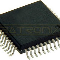
MC68HC705C9ACFBE Freescale Semiconductor, MC68HC705C9ACFBE Datasheet - Page 42

MC68HC705C9ACFBE
Manufacturer Part Number
MC68HC705C9ACFBE
Description
IC MCU 8BIT 44-QFP
Manufacturer
Freescale Semiconductor
Series
HC05r
Datasheet
1.MC705C9ACPE.pdf
(118 pages)
Specifications of MC68HC705C9ACFBE
Core Processor
HC05
Core Size
8-Bit
Speed
2.1MHz
Connectivity
SCI, SPI
Peripherals
POR, WDT
Number Of I /o
24
Program Memory Size
16KB (16K x 8)
Program Memory Type
OTP
Ram Size
352 x 8
Voltage - Supply (vcc/vdd)
3 V ~ 5.5 V
Oscillator Type
Internal
Operating Temperature
-40°C ~ 85°C
Package / Case
44-QFP
Processor Series
HC705C
Core
HC05
Data Bus Width
8 bit
Data Ram Size
352 B
Interface Type
SCI, SPI
Maximum Clock Frequency
2.1 MHz
Number Of Programmable I/os
31
Number Of Timers
1
Maximum Operating Temperature
+ 85 C
Mounting Style
SMD/SMT
Minimum Operating Temperature
- 40 C
On-chip Adc
8 bit
Package
44PQFP
Family Name
HC05
Maximum Speed
2.1 MHz
Operating Supply Voltage
3.3|5 V
Lead Free Status / RoHS Status
Lead free / RoHS Compliant
Eeprom Size
-
Data Converters
-
Lead Free Status / Rohs Status
Details
Available stocks
Company
Part Number
Manufacturer
Quantity
Price
Company:
Part Number:
MC68HC705C9ACFBE
Manufacturer:
FREESCALE
Quantity:
1 827
Company:
Part Number:
MC68HC705C9ACFBE
Manufacturer:
Freescale Semiconductor
Quantity:
10 000
Resets
COPF — Computer Operating Properly Flag
CME — Clock Monitor Enable Bit
COPE — COP Enable Bit
CM1 — COP Mode Bit 1
CM0 — COP Mode Bit 0
Bits 7–5 — Not Used
5.6 MC68HC05C12A Compatible COP
This COP is implemented with an 18-bit ripple counter. This provides a timeout period of 64 milliseconds
at a bus rate (f
re-initialized in the same fashion as a power-on reset or reset.
42
Reading the COP control register clears COPF.
This bit is readable any time, but may be written only once.
This bit is readable any time. COPE, CM1, and CM0 together may be written with a single write, only
once, after reset. This bit is cleared by reset.
Used in conjunction with CM0 to establish the COP timeout period, this bit is readable any time. COPE,
CM1, and CM0 together may be written with a single write, only once, after reset. This bit is cleared by
reset.
Used in conjunction with CM1 to establish the COP timeout period, this bit is readable any time. COPE,
CM1, and CM0 together may be written with a single write, only once, after reset. This bit is cleared by
reset.
These bits always read as 0.
1 = COP or clock monitor reset has occurred.
0 = No COP or clock monitor reset has occurred.
1 = Clock monitor enabled
0 = Clock monitor disabled
1 = COP enabled
0 = COP disabled
op
$001E
Reset:
Read:
Write:
CM1
0
0
1
1
) of 2 MHz. If the COP should time out, a system reset will occur and the device will be
Bit 7
CM0
0
0
0
1
0
1
MC68HC05C9A Advance Information Data Sheet, Rev. 4.1
Figure 5-5. COP Control Register (COPCR)
= Unimplemented
6
0
0
f
op
Table 5-1. COP Timeout Period
/2
15
Divide By
16
64
1
4
5
0
0
COPF
U
4
U = Undetermined
Timeout Period
(f
osc
CME
131.07 ms
524.29 ms
2.097 sec
32.77 ms
3
0
= 2.0 MHz)
COPE
2
0
Timeout Period
(f
CM1
osc
1
0
262.14 ms
1.048 sec
16.38 ms
65.54 ms
= 4.0 MHz)
Freescale Semiconductor
Bit 0
CM0
0


