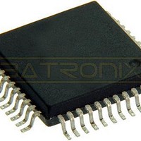
MC68HC705C9ACFBE Freescale Semiconductor, MC68HC705C9ACFBE Datasheet - Page 53

MC68HC705C9ACFBE
Manufacturer Part Number
MC68HC705C9ACFBE
Description
IC MCU 8BIT 44-QFP
Manufacturer
Freescale Semiconductor
Series
HC05r
Datasheet
1.MC705C9ACPE.pdf
(118 pages)
Specifications of MC68HC705C9ACFBE
Core Processor
HC05
Core Size
8-Bit
Speed
2.1MHz
Connectivity
SCI, SPI
Peripherals
POR, WDT
Number Of I /o
24
Program Memory Size
16KB (16K x 8)
Program Memory Type
OTP
Ram Size
352 x 8
Voltage - Supply (vcc/vdd)
3 V ~ 5.5 V
Oscillator Type
Internal
Operating Temperature
-40°C ~ 85°C
Package / Case
44-QFP
Processor Series
HC705C
Core
HC05
Data Bus Width
8 bit
Data Ram Size
352 B
Interface Type
SCI, SPI
Maximum Clock Frequency
2.1 MHz
Number Of Programmable I/os
31
Number Of Timers
1
Maximum Operating Temperature
+ 85 C
Mounting Style
SMD/SMT
Minimum Operating Temperature
- 40 C
On-chip Adc
8 bit
Package
44PQFP
Family Name
HC05
Maximum Speed
2.1 MHz
Operating Supply Voltage
3.3|5 V
Lead Free Status / RoHS Status
Lead free / RoHS Compliant
Eeprom Size
-
Data Converters
-
Lead Free Status / Rohs Status
Details
Available stocks
Company
Part Number
Manufacturer
Quantity
Price
Company:
Part Number:
MC68HC705C9ACFBE
Manufacturer:
FREESCALE
Quantity:
1 827
Company:
Part Number:
MC68HC705C9ACFBE
Manufacturer:
Freescale Semiconductor
Quantity:
10 000
8.3.1 Timer Control Register
The timer control register (TCR), shown in
ICIE — Input Capture Interrupt Enable Bit
OCIE — Output Compare Interrupt Enable Bit
TOIE — Timer Overflow Interrupt Enable Bit
IEDG — Input Edge Bit
OLVL — Output Level Bit
Freescale Semiconductor
•
•
•
•
•
This read/write bit enables interrupts caused by an active signal on the TCAP pin. Resets clear the
ICIE bit.
This read/write bit enables interrupts caused by an active signal on the TCMP pin. Resets clear the
OCIE bit.
This read/write bit enables interrupts caused by a timer overflow. Reset clear the TOIE bit.
The state of this read/write bit determines whether a positive or negative transition on the TCAP pin
triggers a transfer of the contents of the timer register to the input capture register. Resets have no
effect on the IEDG bit.
The state of this read/write bit determines whether a logic 1 or logic 0 appears on the TCMP pin when
a successful output compare occurs. Resets clear the OLVL bit.
1 = Input capture interrupts enabled
0 = Input capture interrupts disabled
1 = Output compare interrupts enabled
0 = Output compare interrupts disabled
1 = Timer overflow interrupts enabled
0 = Timer overflow interrupts disabled
1 = Positive edge (low to high transition) triggers input capture
0 = Negative edge (high to low transition) triggers input capture
1 = TCMP goes high on output compare
0 = TCMP goes low on output compare
Enables input capture interrupts
Enables output compare interrupts
Enables timer overflow interrupts
Controls the active edge polarity of the TCAP signal
Controls the active level of the TCMP output
Reset:
$0012
Read:
Write:
Bit 7
ICIE
0
MC68HC05C9A Advance Information Data Sheet, Rev. 4.1
Figure 8-2. Timer Control Register (TCR)
= Unimplemented
OCIE
6
0
TOIE
5
0
Figure
U = Undetermined
8-2, performs these functions:
4
0
0
3
0
0
2
0
0
IEDG
U
1
OLVL
Bit 0
Timer I/O Registers
0
53


