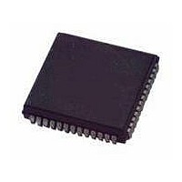
MC68HC11E1VFNE3 Freescale Semiconductor, MC68HC11E1VFNE3 Datasheet - Page 110

MC68HC11E1VFNE3
Manufacturer Part Number
MC68HC11E1VFNE3
Description
MCU 8-BIT 512 RAM 3MHZ 52-PLCC
Manufacturer
Freescale Semiconductor
Series
HC11r
Datasheet
1.MC68HC11E0CFNE2R.pdf
(242 pages)
Specifications of MC68HC11E1VFNE3
Core Processor
HC11
Core Size
8-Bit
Speed
3MHz
Connectivity
SCI, SPI
Peripherals
POR, WDT
Number Of I /o
38
Program Memory Type
ROMless
Eeprom Size
512 x 8
Ram Size
512 x 8
Voltage - Supply (vcc/vdd)
4.5 V ~ 5.5 V
Data Converters
A/D 8x8b
Oscillator Type
Internal
Operating Temperature
-40°C ~ 105°C
Package / Case
52-PLCC
Processor Series
HC11E
Core
HC11
Data Bus Width
8 bit
Data Ram Size
512 B
Interface Type
SCI, SPI
Maximum Clock Frequency
3 MHz
Number Of Programmable I/os
38
Number Of Timers
8
Maximum Operating Temperature
+ 105 C
Mounting Style
SMD/SMT
Minimum Operating Temperature
- 40 C
On-chip Adc
8 bit, 8 Channel
Lead Free Status / RoHS Status
Lead free / RoHS Compliant
Program Memory Size
-
Lead Free Status / Rohs Status
Details
Available stocks
Company
Part Number
Manufacturer
Quantity
Price
Company:
Part Number:
MC68HC11E1VFNE3
Manufacturer:
Freescale Semiconductor
Quantity:
10 000
- Current page: 110 of 242
- Download datasheet (2Mb)
Serial Communications Interface (SCI)
7.7.1 Serial Communications Data Register
SCDR is a parallel register that performs two functions:
Reads access the receive data buffer and writes access the transmit data buffer. Receive and transmit
are double buffered.
7.7.2 Serial Communications Control Register 1
The SCCR1 register provides the control bits that determine word length and select the method used for
the wakeup feature.
R8 — Receive Data Bit 8
T8 — Transmit Data Bit 8
Bit 5 — Unimplemented
M — Mode Bit (select character format)
WAKE — Wakeup by Address Mark/Idle Bit
Bits [2:0] — Unimplemented
110
•
•
If M bit is set, R8 stores the ninth bit in the receive data character.
If M bit is set, T8 stores the ninth bit in the transmit data character.
Always reads 0
Always read 0
0 = Start bit, 8 data bits, 1 stop bit
1 = Start bit, 9 data bits, 1 stop bit
0 = Wakeup by IDLE line recognition
1 = Wakeup by address mark (most significant data bit set)
The receive data register when it is read
The transmit data register when it is written
Address:
Address:
Reset:
Reset:
Read:
Read:
Write:
Write:
Figure 7-4. Serial Communications Control Register 1 (SCCR1)
Figure 7-3. Serial Communications Data Register (SCDR)
I = Indeterminate after reset
$102C
$102F
R7/T7
Bit 7
Bit 7
R8
I
= Unimplemented
R6/T6
T8
6
6
I
M68HC11E Family Data Sheet, Rev. 5.1
R5/T5
5
5
0
Indeterminate after reset
R4/T4
M
4
4
0
WAKE
R3/T3
3
3
0
R2/T2
2
2
0
R1/T1
1
1
0
Freescale Semiconductor
R0/T0
Bit 0
Bit 0
0
Related parts for MC68HC11E1VFNE3
Image
Part Number
Description
Manufacturer
Datasheet
Request
R

Part Number:
Description:
MC68HC11 EEPROM Programming from a Personal Computer
Manufacturer:
Motorola / Freescale Semiconductor
Part Number:
Description:
Manufacturer:
Freescale Semiconductor, Inc
Datasheet:
Part Number:
Description:
Manufacturer:
Freescale Semiconductor, Inc
Datasheet:
Part Number:
Description:
Manufacturer:
Freescale Semiconductor, Inc
Datasheet:
Part Number:
Description:
Manufacturer:
Freescale Semiconductor, Inc
Datasheet:
Part Number:
Description:
Manufacturer:
Freescale Semiconductor, Inc
Datasheet:
Part Number:
Description:
Manufacturer:
Freescale Semiconductor, Inc
Datasheet:
Part Number:
Description:
Manufacturer:
Freescale Semiconductor, Inc
Datasheet:
Part Number:
Description:
Manufacturer:
Freescale Semiconductor, Inc
Datasheet:
Part Number:
Description:
Manufacturer:
Freescale Semiconductor, Inc
Datasheet:
Part Number:
Description:
Manufacturer:
Freescale Semiconductor, Inc
Datasheet:
Part Number:
Description:
Manufacturer:
Freescale Semiconductor, Inc
Datasheet:
Part Number:
Description:
Manufacturer:
Freescale Semiconductor, Inc
Datasheet:
Part Number:
Description:
Manufacturer:
Freescale Semiconductor, Inc
Datasheet:
Part Number:
Description:
Manufacturer:
Freescale Semiconductor, Inc
Datasheet:


