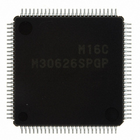
M30626SPGP#U3C Renesas Electronics America, M30626SPGP#U3C Datasheet - Page 148

M30626SPGP#U3C
Manufacturer Part Number
M30626SPGP#U3C
Description
IC M16C/62P MCU ROMLESS 100LQFP
Manufacturer
Renesas Electronics America
Series
M16C™ M16C/60r
Datasheet
1.M30620SPGPU3C.pdf
(423 pages)
Specifications of M30626SPGP#U3C
Core Processor
M16C/60
Core Size
16-Bit
Speed
24MHz
Connectivity
I²C, IEBus, UART/USART
Peripherals
DMA, WDT
Number Of I /o
50
Program Memory Type
ROMless
Ram Size
31K x 8
Voltage - Supply (vcc/vdd)
2.7 V ~ 5.5 V
Data Converters
A/D 26x10b; D/A 2x8b
Oscillator Type
Internal
Operating Temperature
-40°C ~ 85°C
Package / Case
100-LQFP
For Use With
867-1000 - KIT QUICK START RENESAS 62PR0K33062PS001BE - R0K33062P STARTER KITR0K33062PS000BE - KIT EVAL STARTER FOR M16C/62PM3062PT3-CPE-3 - EMULATOR COMPACT M16C/62P/30P
Lead Free Status / RoHS Status
Lead free / RoHS Compliant
Eeprom Size
-
Program Memory Size
-
Available stocks
Company
Part Number
Manufacturer
Quantity
Price
- Current page: 148 of 423
- Download datasheet (5Mb)
M16C/62P Group (M16C/62P, M16C/62PT)
Rev.2.41
REJ09B0185-0241
Figure 14.5
DMAi Destination Pointer (i = 0, 1)
DMAi Transfer Counter (i = 0, 1)
DMAi Source Pointer (i = 0, 1)
(b23)
(b15)
(b23)
b7
b7
NOTES :
b7
NOTES :
1.
1.
If the DAD bit in the DMiCON register is “0” (fixed), this register can only be w ritten to w hen the DMAE bit in the
DMiCON register is “0”(DMA disabled).
If the DAD bit is “1” (forw ard direction), this register can be w ritten to at any time.
If the DAD bit is “1” and the DMAE bit is “1” (DMA enabled), the DMAi forw ard address pointer can be read from this
register. Otherw ise, the value w ritten to it can be read.
If the DSD bit in the DMiCON register is “0” (fixed), this register can only be w ritten to w hen the DMAE bit in the
DMiCON register is “0” (DMA disabled).
If the DSD bit is “1” (forw ard direction), this register can be w ritten to at any time.
If the DSD bit is “1” and the DMAE bit is “1” (DMA enabled), the DMAi forw ard address pointer can be read from this
register. Otherw ise, the value w ritten to it can be read.
Jan 10, 2006
(b19)
(b19)
b3
b3
SAR0, SAR1, DAR0, DAR1, TCR0 and TCR1 Registers
(b16)
(b16)
(b8)
b0
b0
b0
b7
(b15)
b7
(b15)
b7
Set the destination address of transfer
Nothing is assigned. When w rite, set “0”.
When read, their contents are “0”.
Set the source address of transfer
Nothing is assigned. When w rite, set “0”.
When read, their contents are “0”.
Set the transfer count minus 1. The w ritten value is stored in the DMAi
transfer counter reload register, and w hen the DMAE bit in the DMiCON
register is set to “1” (DMA enabled) or the DMAi transfer counter
underflow s w hen the DMASL bit in the DMiCON register is “1” (repeat
transfer), the value of the DMAi transfer counter reload register is
transferred to the DMAi transfer counter.
When read, the DMAi transfer counter is read.
Page 131 of 390
(1)
(b8)
(b8)
b0
b0 b7
b0
(1)
b7
Symbol
TCR0
TCR1
Function
Function
Function
b0
b0
Symbol
Symbol
DAR0
DAR1
SAR0
SAR1
0029h to 0028h
0039h to 0038h
Address
0022h to 0020h
0032h to 0030h
0026h to 0024h
0036h to 0034h
Address
Address
00000h to FFFFFh
00000h to FFFFFh
0000h to FFFFh
Setting Range
Indeterminate
Indeterminate
Setting Range
Indeterminate
Indeterminate
Setting Range
Indeterminate
Indeterminate
After Reset
After Reset
After Reset
14. DMAC
RW
RW
RW
RW
RW
RW
—
—
Related parts for M30626SPGP#U3C
Image
Part Number
Description
Manufacturer
Datasheet
Request
R

Part Number:
Description:
KIT STARTER FOR M16C/29
Manufacturer:
Renesas Electronics America
Datasheet:

Part Number:
Description:
KIT STARTER FOR R8C/2D
Manufacturer:
Renesas Electronics America
Datasheet:

Part Number:
Description:
R0K33062P STARTER KIT
Manufacturer:
Renesas Electronics America
Datasheet:

Part Number:
Description:
KIT STARTER FOR R8C/23 E8A
Manufacturer:
Renesas Electronics America
Datasheet:

Part Number:
Description:
KIT STARTER FOR R8C/25
Manufacturer:
Renesas Electronics America
Datasheet:

Part Number:
Description:
KIT STARTER H8S2456 SHARPE DSPLY
Manufacturer:
Renesas Electronics America
Datasheet:

Part Number:
Description:
KIT STARTER FOR R8C38C
Manufacturer:
Renesas Electronics America
Datasheet:

Part Number:
Description:
KIT STARTER FOR R8C35C
Manufacturer:
Renesas Electronics America
Datasheet:

Part Number:
Description:
KIT STARTER FOR R8CL3AC+LCD APPS
Manufacturer:
Renesas Electronics America
Datasheet:

Part Number:
Description:
KIT STARTER FOR RX610
Manufacturer:
Renesas Electronics America
Datasheet:

Part Number:
Description:
KIT STARTER FOR R32C/118
Manufacturer:
Renesas Electronics America
Datasheet:

Part Number:
Description:
KIT DEV RSK-R8C/26-29
Manufacturer:
Renesas Electronics America
Datasheet:

Part Number:
Description:
KIT STARTER FOR SH7124
Manufacturer:
Renesas Electronics America
Datasheet:

Part Number:
Description:
KIT STARTER FOR H8SX/1622
Manufacturer:
Renesas Electronics America
Datasheet:

Part Number:
Description:
KIT DEV FOR SH7203
Manufacturer:
Renesas Electronics America
Datasheet:


