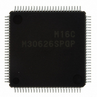
M30626SPGP#U3C Renesas Electronics America, M30626SPGP#U3C Datasheet - Page 253

M30626SPGP#U3C
Manufacturer Part Number
M30626SPGP#U3C
Description
IC M16C/62P MCU ROMLESS 100LQFP
Manufacturer
Renesas Electronics America
Series
M16C™ M16C/60r
Datasheet
1.M30620SPGPU3C.pdf
(423 pages)
Specifications of M30626SPGP#U3C
Core Processor
M16C/60
Core Size
16-Bit
Speed
24MHz
Connectivity
I²C, IEBus, UART/USART
Peripherals
DMA, WDT
Number Of I /o
50
Program Memory Type
ROMless
Ram Size
31K x 8
Voltage - Supply (vcc/vdd)
2.7 V ~ 5.5 V
Data Converters
A/D 26x10b; D/A 2x8b
Oscillator Type
Internal
Operating Temperature
-40°C ~ 85°C
Package / Case
100-LQFP
For Use With
867-1000 - KIT QUICK START RENESAS 62PR0K33062PS001BE - R0K33062P STARTER KITR0K33062PS000BE - KIT EVAL STARTER FOR M16C/62PM3062PT3-CPE-3 - EMULATOR COMPACT M16C/62P/30P
Lead Free Status / RoHS Status
Lead free / RoHS Compliant
Eeprom Size
-
Program Memory Size
-
Available stocks
Company
Part Number
Manufacturer
Quantity
Price
- Current page: 253 of 423
- Download datasheet (5Mb)
M16C/62P Group (M16C/62P, M16C/62PT)
Rev.2.41
REJ09B0185-0241
Figure 18.3
A/D Control Register 2
b7 b6 b5 b4 b3 b2 b1 b0
NOTES :
1.
2.
3.
If the ADCON2 register is rew ritten during A/D conversion, the conversion result w ill be indeterminate.
If VCC2 < VCC1, do not use AN0_0 to AN0_7 and AN2_0 to AN2_7 as analog input pins.
The ØAD frequency must be 12 MHz or less. The selected ØAD frequency is determined by a combination of the CKS0
bit in the ADCON0 register, the CKS1 bit in the ADCON1 register, and the CKS2 bit in the ADCON2 register.
Jan 10, 2006
CKS2
0
0
0
0
0
1
1
1
1
ADCON2 Register
Bit Symbol
ADGSEL0
ADGSEL1
ADCON2
(b7-b5)
Symbol
CKS1
CKS2
(1)
SMP
(b3)
0
0
1
1
0
0
1
1
—
—
Page 236 of 390
A/D Conversion Method Select
Bit
A/D Input Group Select Bit
Reserved Bit
Frequency Select Bit 2
Nothing is assigned.
When w rite, set to “0”. When read, their contents are “0”.
CKS0
0
1
0
1
0
1
0
1
Address
Bit Name
03D4h
Divide-by-4 of fAD
Divide-by-2 of fAD
fAD
Ddivide-by-12 of fAD
Divide-by-6 of fAD
Divide-by-3 of fAD
(3)
ØAD
b2 b1
0 0 : Port P10 group is selected
0 1 : Do not set
1 0 : Port P0 group is selected
1 1 : Port P2 group is selected
0 : Without sample and hold
1 : With sample and hold
Set to “0”
0: Selects fAD, fAD divided by 2, or fAD
1: Selects fAD divided by 3, fAD divided
divided by 4.
by 6, or fAD divided by 12.
After Reset
Function
00h
(2)
18. A/D Converter
RW
RW
RW
RW
RW
RW
—
Related parts for M30626SPGP#U3C
Image
Part Number
Description
Manufacturer
Datasheet
Request
R

Part Number:
Description:
KIT STARTER FOR M16C/29
Manufacturer:
Renesas Electronics America
Datasheet:

Part Number:
Description:
KIT STARTER FOR R8C/2D
Manufacturer:
Renesas Electronics America
Datasheet:

Part Number:
Description:
R0K33062P STARTER KIT
Manufacturer:
Renesas Electronics America
Datasheet:

Part Number:
Description:
KIT STARTER FOR R8C/23 E8A
Manufacturer:
Renesas Electronics America
Datasheet:

Part Number:
Description:
KIT STARTER FOR R8C/25
Manufacturer:
Renesas Electronics America
Datasheet:

Part Number:
Description:
KIT STARTER H8S2456 SHARPE DSPLY
Manufacturer:
Renesas Electronics America
Datasheet:

Part Number:
Description:
KIT STARTER FOR R8C38C
Manufacturer:
Renesas Electronics America
Datasheet:

Part Number:
Description:
KIT STARTER FOR R8C35C
Manufacturer:
Renesas Electronics America
Datasheet:

Part Number:
Description:
KIT STARTER FOR R8CL3AC+LCD APPS
Manufacturer:
Renesas Electronics America
Datasheet:

Part Number:
Description:
KIT STARTER FOR RX610
Manufacturer:
Renesas Electronics America
Datasheet:

Part Number:
Description:
KIT STARTER FOR R32C/118
Manufacturer:
Renesas Electronics America
Datasheet:

Part Number:
Description:
KIT DEV RSK-R8C/26-29
Manufacturer:
Renesas Electronics America
Datasheet:

Part Number:
Description:
KIT STARTER FOR SH7124
Manufacturer:
Renesas Electronics America
Datasheet:

Part Number:
Description:
KIT STARTER FOR H8SX/1622
Manufacturer:
Renesas Electronics America
Datasheet:

Part Number:
Description:
KIT DEV FOR SH7203
Manufacturer:
Renesas Electronics America
Datasheet:


