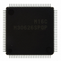
M30626SPGP#U3C Renesas Electronics America, M30626SPGP#U3C Datasheet - Page 260

M30626SPGP#U3C
Manufacturer Part Number
M30626SPGP#U3C
Description
IC M16C/62P MCU ROMLESS 100LQFP
Manufacturer
Renesas Electronics America
Series
M16C™ M16C/60r
Datasheet
1.M30620SPGPU3C.pdf
(423 pages)
Specifications of M30626SPGP#U3C
Core Processor
M16C/60
Core Size
16-Bit
Speed
24MHz
Connectivity
I²C, IEBus, UART/USART
Peripherals
DMA, WDT
Number Of I /o
50
Program Memory Type
ROMless
Ram Size
31K x 8
Voltage - Supply (vcc/vdd)
2.7 V ~ 5.5 V
Data Converters
A/D 26x10b; D/A 2x8b
Oscillator Type
Internal
Operating Temperature
-40°C ~ 85°C
Package / Case
100-LQFP
For Use With
867-1000 - KIT QUICK START RENESAS 62PR0K33062PS001BE - R0K33062P STARTER KITR0K33062PS000BE - KIT EVAL STARTER FOR M16C/62PM3062PT3-CPE-3 - EMULATOR COMPACT M16C/62P/30P
Lead Free Status / RoHS Status
Lead free / RoHS Compliant
Eeprom Size
-
Program Memory Size
-
Available stocks
Company
Part Number
Manufacturer
Quantity
Price
- Current page: 260 of 423
- Download datasheet (5Mb)
M16C/62P Group (M16C/62P, M16C/62PT)
Rev.2.41
REJ09B0185-0241
Figure 18.7
A/D Control Register 1
A/D Control Register 0
b7 b6 b5 b4
NOTES :
b7 b6 b5 b4 b3 b2 b1 b0
NOTES :
1. If the ADCON0 register is rew ritten during A/D conversion, the conversion result w ill be indeterminate.
1.
2.
3.
1
If the ADCON1 register is rew ritten during A/D conversion, the conversion result w ill be indeterminate.
AN0_0 to AN0_7, and AN2_0 to AN2_7 can be used in the same w ay as AN0 to AN7. Use the ADGSEL1 to
ADGSEL0 bits in the ADCON2 register to select the desired pin. How ever, if VCC2 < VCC1, do not use AN0_0 to
AN0_7 and AN2_0 to AN2_7 as analog input pins.
If the VCUT bit is reset from “0” (Vref unconnected) to “1” (Vref connected), w ait for 1 µs or more before starting
A/D conversion.
Jan 10, 2006
1 0
b3 b2 b1 b0
0
ADCON0 Register and ADCON1 Register (Single Sweep Mode)
Bit Symbol
ADCON1
ADCON0
SCAN0
SCAN1
Symbol
Symbol
Symbol
CKS1
VCUT
OPA0
OPA1
ADST
CKS0
MD2
BITS
MD1
TRG
(1)
(1)
CH0
CH1
CH2
MD0
Page 243 of 390
Analog Input Pin Select Bit
A/D Operation Mode Select
Bit 0
Trigger Select Bit
A/D Conversion Start Flag
Frequency Select Bit 0
A/D Sw eep Pin Select Bit
A/D Operation Mode Select Bit 1 Set to “0” w hen single sw eep mode is selected
8/10-Bit Mode Select Bit
Frequency Select Bit 1
Vref Connect Bit
External Op-Amp Connection
Mode Bit
Address
Bit Name
Address
Address
03D7h
03D6h
(3)
(2)
b4 b3
1 0 : Single sw eep mode
b7 b6
0 0 : ANEX0 and ANEX1 are not used
0 1 : Do not set to this value
1 0 : Do not set to this value
1 1 : External op-amp connection mode
When single sw eep mode is selected
b1 b0
0 0 : AN0 to AN1 (2 pins)
0 1 : AN0 to AN3 (4 pins)
1 0 : AN0 to AN5 (6 pins)
1 1 : AN0 to AN7 (8 pins)
0 : 8-bit mode
1 : 10-bit mode
Refer to NOTE 3 for the ADCON2 Register
1 : Vref connected
Invalid in single sw eep mode
0 : Softw are trigger
1 : ADTRG
0 : A/D conversion disabled
1 : A/D conversion started
Refer to NOTE 3 for the ADCON2 Register
_________
trigger
00000XXXb
After Reset
After Reset
After Reset
Function
00h
18. A/D Converter
RW
RW
RW
RW
RW
RW
RW
RW
RW
RW
RW
RW
RW
RW
RW
RW
RW
RW
Related parts for M30626SPGP#U3C
Image
Part Number
Description
Manufacturer
Datasheet
Request
R

Part Number:
Description:
KIT STARTER FOR M16C/29
Manufacturer:
Renesas Electronics America
Datasheet:

Part Number:
Description:
KIT STARTER FOR R8C/2D
Manufacturer:
Renesas Electronics America
Datasheet:

Part Number:
Description:
R0K33062P STARTER KIT
Manufacturer:
Renesas Electronics America
Datasheet:

Part Number:
Description:
KIT STARTER FOR R8C/23 E8A
Manufacturer:
Renesas Electronics America
Datasheet:

Part Number:
Description:
KIT STARTER FOR R8C/25
Manufacturer:
Renesas Electronics America
Datasheet:

Part Number:
Description:
KIT STARTER H8S2456 SHARPE DSPLY
Manufacturer:
Renesas Electronics America
Datasheet:

Part Number:
Description:
KIT STARTER FOR R8C38C
Manufacturer:
Renesas Electronics America
Datasheet:

Part Number:
Description:
KIT STARTER FOR R8C35C
Manufacturer:
Renesas Electronics America
Datasheet:

Part Number:
Description:
KIT STARTER FOR R8CL3AC+LCD APPS
Manufacturer:
Renesas Electronics America
Datasheet:

Part Number:
Description:
KIT STARTER FOR RX610
Manufacturer:
Renesas Electronics America
Datasheet:

Part Number:
Description:
KIT STARTER FOR R32C/118
Manufacturer:
Renesas Electronics America
Datasheet:

Part Number:
Description:
KIT DEV RSK-R8C/26-29
Manufacturer:
Renesas Electronics America
Datasheet:

Part Number:
Description:
KIT STARTER FOR SH7124
Manufacturer:
Renesas Electronics America
Datasheet:

Part Number:
Description:
KIT STARTER FOR H8SX/1622
Manufacturer:
Renesas Electronics America
Datasheet:

Part Number:
Description:
KIT DEV FOR SH7203
Manufacturer:
Renesas Electronics America
Datasheet:


