M30626SPGP#U3C Renesas Electronics America, M30626SPGP#U3C Datasheet - Page 296
M30626SPGP#U3C
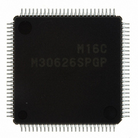
Manufacturer Part Number
M30626SPGP#U3C
Description
IC M16C/62P MCU ROMLESS 100LQFP
Manufacturer
Renesas Electronics America
Series
M16C™ M16C/60r
Datasheet
1.M30620SPGPU3C.pdf
(423 pages)
Specifications of M30626SPGP#U3C
Core Processor
M16C/60
Core Size
16-Bit
Speed
24MHz
Connectivity
I²C, IEBus, UART/USART
Peripherals
DMA, WDT
Number Of I /o
50
Program Memory Type
ROMless
Ram Size
31K x 8
Voltage - Supply (vcc/vdd)
2.7 V ~ 5.5 V
Data Converters
A/D 26x10b; D/A 2x8b
Oscillator Type
Internal
Operating Temperature
-40°C ~ 85°C
Package / Case
100-LQFP
For Use With
867-1000 - KIT QUICK START RENESAS 62PR0K33062PS001BE - R0K33062P STARTER KITR0K33062PS000BE - KIT EVAL STARTER FOR M16C/62PM3062PT3-CPE-3 - EMULATOR COMPACT M16C/62P/30P
Lead Free Status / RoHS Status
Lead free / RoHS Compliant
Eeprom Size
-
Program Memory Size
-
Available stocks
Company
Part Number
Manufacturer
Quantity
Price


M16C/62P Group (M16C/62P, M16C/62PT)
Rev.2.41
REJ09B0185-0241
22.3.3.1
22.3.3.2
22.3.3.3
22.3.3.4
22.3.3.5
This bit indicates the flash memory operating state. It is set to “0” while the program, block erase, erase all
unlocked block, lock bit program, or read lock bit status command is being executed; otherwise, it is set to “1”.
The microcomputer can accept commands when the FMR01 bit is set to “1” (CPU rewrite mode). Set the
FMR05 bit to “1” (user ROM area access) as well if in boot mode.
The lock bit is disabled by setting the FMR02 bit to “1” (lock bit disabled). (Refer to 22.3.6 Data Protect
Function.) The lock bit is enabled by setting the FMR02 bit to “0” (lock bit enabled).
The FMR02 bit does not change the lock bit status but disables the lock bit function. If the block erase or erase
all unlocked block command is executed when the FMR02 bit is set to “1”, the lock bit status changes “0”
(locked) to “1” (unlocked) after command execution is completed.
The FMSTP bit resets the flash memory control circuits and minimizes power consumption in the flash
memory. Access to the flash memory is disabled when the FMSTP bit is set to “1”. Set the FMSTP bit by
program in a space other than the flash memory.
Use the following the procedure to change the FMSTP bit setting.
Figure 22.9 shows a Flow Chart Illustrating How To Start and Stop the Flash Memory Processing Before and
After Low Power Dissipation Mode or On-chip Oscillator Low-Power Consumption Mode. Follow the
procedure on this flow chart.
When entering stop or wait mode, the flash memory is automatically turned off. When exiting stop or wait
mode, the flash memory is turned back on. The FMR0 register does not need to be set.
This bit selects the boot ROM or user ROM area in boot mode. Set to “0” to access (read) the boot ROM area or
to “1” (user ROM access) to access (read, write or erase) the user ROM area.
•
•
(1) Set the FMSTP bit to “1”
(2) Set tps (the wait time to stabilize flash memory circuit)
(3) Set the FMSTP bit to “0”
(4) Set tps (the wait time to stabilize flash memory circuit)
Jan 10, 2006
Set the FMSTP bit to “1” if one of the followings occurs: A flash memory access error occurs while erasing
or programming in EW0 mode (FMR00 bit does not switch back to “1” (ready)).
Low-power consumption mode or on-chip oscillator low-power consumption mode is entered
FMR00 Bit
FMR01 Bit
FMR02 Bit
FMSTP Bit
FMR05 Bit
Page 279 of 390
22. Flash Memory Version
Related parts for M30626SPGP#U3C
Image
Part Number
Description
Manufacturer
Datasheet
Request
R

Part Number:
Description:
KIT STARTER FOR M16C/29
Manufacturer:
Renesas Electronics America
Datasheet:

Part Number:
Description:
KIT STARTER FOR R8C/2D
Manufacturer:
Renesas Electronics America
Datasheet:

Part Number:
Description:
R0K33062P STARTER KIT
Manufacturer:
Renesas Electronics America
Datasheet:

Part Number:
Description:
KIT STARTER FOR R8C/23 E8A
Manufacturer:
Renesas Electronics America
Datasheet:

Part Number:
Description:
KIT STARTER FOR R8C/25
Manufacturer:
Renesas Electronics America
Datasheet:

Part Number:
Description:
KIT STARTER H8S2456 SHARPE DSPLY
Manufacturer:
Renesas Electronics America
Datasheet:

Part Number:
Description:
KIT STARTER FOR R8C38C
Manufacturer:
Renesas Electronics America
Datasheet:

Part Number:
Description:
KIT STARTER FOR R8C35C
Manufacturer:
Renesas Electronics America
Datasheet:

Part Number:
Description:
KIT STARTER FOR R8CL3AC+LCD APPS
Manufacturer:
Renesas Electronics America
Datasheet:
Part Number:
Description:
KIT STARTER FOR RX610
Manufacturer:
Renesas Electronics America
Datasheet:

Part Number:
Description:
KIT STARTER FOR R32C/118
Manufacturer:
Renesas Electronics America
Datasheet:

Part Number:
Description:
KIT DEV RSK-R8C/26-29
Manufacturer:
Renesas Electronics America
Datasheet:

Part Number:
Description:
KIT STARTER FOR SH7124
Manufacturer:
Renesas Electronics America
Datasheet:

Part Number:
Description:
KIT STARTER FOR H8SX/1622
Manufacturer:
Renesas Electronics America
Datasheet:

Part Number:
Description:
KIT DEV FOR SH7203
Manufacturer:
Renesas Electronics America
Datasheet: