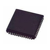
MC68HC711E9VFNE2 Freescale Semiconductor, MC68HC711E9VFNE2 Datasheet - Page 100

MC68HC711E9VFNE2
Manufacturer Part Number
MC68HC711E9VFNE2
Description
IC MCU 8BIT 512BYTES ROM 52-PLCC
Manufacturer
Freescale Semiconductor
Series
HC11r
Specifications of MC68HC711E9VFNE2
Core Processor
HC11
Core Size
8-Bit
Speed
2MHz
Connectivity
SCI, SPI
Peripherals
POR, WDT
Number Of I /o
38
Program Memory Size
12KB (12K x 8)
Program Memory Type
OTP
Eeprom Size
512 x 8
Ram Size
512 x 8
Voltage - Supply (vcc/vdd)
4.5 V ~ 5.5 V
Data Converters
A/D 8x8b
Oscillator Type
Internal
Operating Temperature
-40°C ~ 105°C
Package / Case
52-PLCC
Processor Series
HC711E
Core
HC11
Data Bus Width
8 bit
Data Ram Size
512 B
Interface Type
SCI, SPI
Maximum Clock Frequency
2 MHz
Number Of Programmable I/os
38
Number Of Timers
8
Maximum Operating Temperature
+ 105 C
Mounting Style
SMD/SMT
Minimum Operating Temperature
- 40 C
On-chip Adc
8 bit
Lead Free Status / RoHS Status
Lead free / RoHS Compliant
Available stocks
Company
Part Number
Manufacturer
Quantity
Price
Company:
Part Number:
MC68HC711E9VFNE2
Manufacturer:
Freescale Semiconductor
Quantity:
10 000
- Current page: 100 of 242
- Download datasheet (2Mb)
PORTCL is used in the handshake clearing mechanism. When an active edge occurs on the STRA pin,
port C data is latched into the PORTCL register. Reads of this register return the last value latched into
PORTCL and clear STAF flag (following a read of PIOC with STAF set).
DDRC[7:0] — Port C Data Direction Bits
6.5 Port D
In all modes, port D bits [5:0] can be used either for general-purpose I/O or with the serial communications
interface (SCI) and serial peripheral interface (SPI) subsystems. During reset, port D pins PD[5:0] are
configured as high-impedance inputs (DDRD bits cleared).
Bits [7:6] — Unimplemented
DDRD[5:0] — Port D Data Direction Bits
100
Parallel Input/Output (I/O) Ports
In the 3-state variation of output handshake mode, clear the corresponding DDRC bits. Refer to
10-13. 3-State Variation of Output Handshake Timing Diagram (STRA Enables Output
Always read 0
When DDRD bit 5 is 1 and MSTR = 1 in SPCR, PD5/SS is a general-purpose output and mode fault
logic is disabled.
0 = Input
1 = Output
0 = Input
1 = Output
Alternate Function:
Address:
Address:
Reset:
Reset:
Read:
Read:
Write:
Write:
Address:
Reset:
Read:
Write:
DDRC7
$1007
$1009
Bit 7
Bit 7
I = Indeterminate after reset
0
0
Figure 6-6. Port C Data Direction Register (DDRC)
Figure 6-8. Port D Data Direction Register (DDRD)
$1008
Bit 7
—
—
0
Figure 6-7. Port D Data Register (PORTD)
= Unimplemented
DDRC6
6
0
6
0
M68HC11E Family Data Sheet, Rev. 5.1
—
—
6
0
DDRC5
DDRD5
5
0
5
0
PD5
PD5
SS
5
I
DDRC4
DDRD4
4
0
4
0
SCK
PD4
PD4
4
I
DDRC3
DDRD3
3
0
3
0
MOSI
PD3
PD3
3
I
DDRC2
DDRD2
2
0
2
0
MISO
PD2
PD2
2
I
DDRC1
DDRD1
1
0
1
0
PD1
PD1
Tx
1
I
Freescale Semiconductor
DDRC0
DDRD0
Bit 0
Bit 0
0
0
Bit 0
PD0
PD0
RxD
Buffer).
I
Figure
Related parts for MC68HC711E9VFNE2
Image
Part Number
Description
Manufacturer
Datasheet
Request
R

Part Number:
Description:
APPENDIX A ELECTRICAL CHARACTERISTICS
Manufacturer:
FREESCALE [Freescale Semiconductor, Inc]
Datasheet:
Part Number:
Description:
Manufacturer:
Freescale Semiconductor, Inc
Datasheet:
Part Number:
Description:
Manufacturer:
Freescale Semiconductor, Inc
Datasheet:
Part Number:
Description:
Manufacturer:
Freescale Semiconductor, Inc
Datasheet:
Part Number:
Description:
Manufacturer:
Freescale Semiconductor, Inc
Datasheet:
Part Number:
Description:
Manufacturer:
Freescale Semiconductor, Inc
Datasheet:
Part Number:
Description:
Manufacturer:
Freescale Semiconductor, Inc
Datasheet:
Part Number:
Description:
Manufacturer:
Freescale Semiconductor, Inc
Datasheet:
Part Number:
Description:
Manufacturer:
Freescale Semiconductor, Inc
Datasheet:
Part Number:
Description:
Manufacturer:
Freescale Semiconductor, Inc
Datasheet:
Part Number:
Description:
Manufacturer:
Freescale Semiconductor, Inc
Datasheet:
Part Number:
Description:
Manufacturer:
Freescale Semiconductor, Inc
Datasheet:
Part Number:
Description:
Manufacturer:
Freescale Semiconductor, Inc
Datasheet:
Part Number:
Description:
Manufacturer:
Freescale Semiconductor, Inc
Datasheet:
Part Number:
Description:
Manufacturer:
Freescale Semiconductor, Inc
Datasheet:


