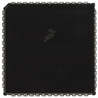
MC68HC711E9CFNE2 Freescale Semiconductor, MC68HC711E9CFNE2 Datasheet - Page 122

MC68HC711E9CFNE2
Manufacturer Part Number
MC68HC711E9CFNE2
Description
IC MCU 8BIT 512RAM 52-PLC
Manufacturer
Freescale Semiconductor
Series
HC11r
Datasheet
1.MC68HC711E9CFNE3.pdf
(336 pages)
Specifications of MC68HC711E9CFNE2
Core Processor
HC11
Core Size
8-Bit
Speed
2MHz
Connectivity
SCI, SPI
Peripherals
POR, WDT
Number Of I /o
38
Program Memory Size
12KB (12K x 8)
Program Memory Type
OTP
Eeprom Size
512 x 8
Ram Size
512 x 8
Voltage - Supply (vcc/vdd)
4.5 V ~ 5.5 V
Data Converters
A/D 8x8b
Oscillator Type
Internal
Operating Temperature
-40°C ~ 85°C
Package / Case
52-PLCC
Processor Series
HC711E
Core
HC11
Data Bus Width
8 bit
Data Ram Size
512 B
Interface Type
SCI, SPI
Maximum Clock Frequency
2 MHz
Number Of Programmable I/os
38
Number Of Timers
8
Maximum Operating Temperature
+ 85 C
Mounting Style
SMD/SMT
Minimum Operating Temperature
- 40 C
On-chip Adc
8 bit
Lead Free Status / RoHS Status
Lead free / RoHS Compliant
Available stocks
Company
Part Number
Manufacturer
Quantity
Price
Company:
Part Number:
MC68HC711E9CFNE2
Manufacturer:
TE
Quantity:
12 000
Company:
Part Number:
MC68HC711E9CFNE2
Manufacturer:
FREESCAL
Quantity:
5 530
- Current page: 122 of 336
- Download datasheet (4Mb)
Resets and Interrupts
5.6.1 Interrupt Recognition and Register Stacking
Technical Data
122
For some interrupt sources, such as the SCI interrupts, the flags are
automatically cleared during the normal course of responding to the
interrupt requests. For example, the RDRF flag in the SCI system is
cleared by the automatic clearing mechanism consisting of a read of the
SCI status register while RDRF is set, followed by a read of the SCI data
register. The normal response to an RDRF interrupt request would be to
read the SCI status register to check for receive errors, then to read the
received data from the SCI data register. These steps satisfy the
automatic clearing mechanism without requiring special instructions.
An interrupt can be recognized at any time after it is enabled by its local
mask, if any, and by the global mask bit in the CCR. Once an interrupt
source is recognized, the CPU responds at the completion of the
instruction being executed. Interrupt latency varies according to the
number of cycles required to complete the current instruction. When the
CPU begins to service an interrupt, the contents of the CPU registers are
pushed onto the stack in the order shown in
value is stacked, the I bit and the X bit, if XIRQ is pending, are set to
inhibit further interrupts. The interrupt vector for the highest priority
pending source is fetched and execution continues at the address
specified by the vector. At the end of the interrupt service routine, the
return-from-interrupt instruction is executed and the saved registers are
pulled from the stack in reverse order so that normal program execution
can resume. Refer to
Table 5-5. Stacking Order on Entry to Interrupts
Memory Location
Resets and Interrupts
SP–1
SP–2
SP–3
SP–4
SP–5
SP–6
SP–7
SP–8
SP
Section 3. Central Processor Unit
CPU Registers
Table
M68HC11E Family — Rev. 3.2
ACCA
ACCB
CCR
PCH
PCL
IYH
IXH
IYL
IXL
5-5. After the CCR
(CPU).
MOTOROLA
Related parts for MC68HC711E9CFNE2
Image
Part Number
Description
Manufacturer
Datasheet
Request
R

Part Number:
Description:
APPENDIX A ELECTRICAL CHARACTERISTICS
Manufacturer:
FREESCALE [Freescale Semiconductor, Inc]
Datasheet:
Part Number:
Description:
Manufacturer:
Freescale Semiconductor, Inc
Datasheet:
Part Number:
Description:
Manufacturer:
Freescale Semiconductor, Inc
Datasheet:
Part Number:
Description:
Manufacturer:
Freescale Semiconductor, Inc
Datasheet:
Part Number:
Description:
Manufacturer:
Freescale Semiconductor, Inc
Datasheet:
Part Number:
Description:
Manufacturer:
Freescale Semiconductor, Inc
Datasheet:
Part Number:
Description:
Manufacturer:
Freescale Semiconductor, Inc
Datasheet:
Part Number:
Description:
Manufacturer:
Freescale Semiconductor, Inc
Datasheet:
Part Number:
Description:
Manufacturer:
Freescale Semiconductor, Inc
Datasheet:
Part Number:
Description:
Manufacturer:
Freescale Semiconductor, Inc
Datasheet:
Part Number:
Description:
Manufacturer:
Freescale Semiconductor, Inc
Datasheet:
Part Number:
Description:
Manufacturer:
Freescale Semiconductor, Inc
Datasheet:
Part Number:
Description:
Manufacturer:
Freescale Semiconductor, Inc
Datasheet:
Part Number:
Description:
Manufacturer:
Freescale Semiconductor, Inc
Datasheet:
Part Number:
Description:
Manufacturer:
Freescale Semiconductor, Inc
Datasheet:


