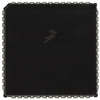
MC68HC711E9CFNE2 Freescale Semiconductor, MC68HC711E9CFNE2 Datasheet - Page 146

MC68HC711E9CFNE2
Manufacturer Part Number
MC68HC711E9CFNE2
Description
IC MCU 8BIT 512RAM 52-PLC
Manufacturer
Freescale Semiconductor
Series
HC11r
Datasheet
1.MC68HC711E9CFNE3.pdf
(336 pages)
Specifications of MC68HC711E9CFNE2
Core Processor
HC11
Core Size
8-Bit
Speed
2MHz
Connectivity
SCI, SPI
Peripherals
POR, WDT
Number Of I /o
38
Program Memory Size
12KB (12K x 8)
Program Memory Type
OTP
Eeprom Size
512 x 8
Ram Size
512 x 8
Voltage - Supply (vcc/vdd)
4.5 V ~ 5.5 V
Data Converters
A/D 8x8b
Oscillator Type
Internal
Operating Temperature
-40°C ~ 85°C
Package / Case
52-PLCC
Processor Series
HC711E
Core
HC11
Data Bus Width
8 bit
Data Ram Size
512 B
Interface Type
SCI, SPI
Maximum Clock Frequency
2 MHz
Number Of Programmable I/os
38
Number Of Timers
8
Maximum Operating Temperature
+ 85 C
Mounting Style
SMD/SMT
Minimum Operating Temperature
- 40 C
On-chip Adc
8 bit
Lead Free Status / RoHS Status
Lead free / RoHS Compliant
Available stocks
Company
Part Number
Manufacturer
Quantity
Price
Company:
Part Number:
MC68HC711E9CFNE2
Manufacturer:
TE
Quantity:
12 000
Company:
Part Number:
MC68HC711E9CFNE2
Manufacturer:
FREESCAL
Quantity:
5 530
- Current page: 146 of 336
- Download datasheet (4Mb)
Serial Communications Interface (SCI)
7.3 Data Format
7.4 Transmit Operation
Technical Data
146
transmitter and receiver are independent, but use the same data format
and bit rate.
All members of the E series contain the same SCI, with one exception.
The SCI system in the MC68HC11E20 and MC68HC711E20 MCUs
have an enhanced SCI baud rate generator. A divide-by-39 stage has
been added that is enabled by an extra bit in the BAUD register. This
increases the available SCI baud rate selections. Refer to
and
The serial data format requires these conditions:
Selection of the word length is controlled by the M bit of SCI control
register (SCCR1).
The SCI transmitter includes a parallel transmit data register (SCDR)
and a serial shift register. The contents of the serial shift register can be
written only through the SCDR. This double buffered operation allows a
character to be shifted out serially while another character is waiting in
the SCDR to be transferred into the serial shift register. The output of the
serial shift register is applied to TxD as long as transmission is in
1. An idle line in the high state before transmission or reception of a
2. A start bit, logic 0, transmitted or received, that indicates the start
3. Data that is transmitted and received least significant bit (LSB) first
4. A stop bit, logic 1, used to indicate the end of a frame. A frame
5. A break, defined as the transmission or reception of a logic 0 for
7.8.5 Baud Rate
message
of each character
consists of a start bit, a character of eight or nine data bits, and a
stop bit.
some multiple number of frames
Serial Communications Interface (SCI)
Register.
M68HC11E Family — Rev. 3.2
Figure 7-8
MOTOROLA
Related parts for MC68HC711E9CFNE2
Image
Part Number
Description
Manufacturer
Datasheet
Request
R

Part Number:
Description:
APPENDIX A ELECTRICAL CHARACTERISTICS
Manufacturer:
FREESCALE [Freescale Semiconductor, Inc]
Datasheet:
Part Number:
Description:
Manufacturer:
Freescale Semiconductor, Inc
Datasheet:
Part Number:
Description:
Manufacturer:
Freescale Semiconductor, Inc
Datasheet:
Part Number:
Description:
Manufacturer:
Freescale Semiconductor, Inc
Datasheet:
Part Number:
Description:
Manufacturer:
Freescale Semiconductor, Inc
Datasheet:
Part Number:
Description:
Manufacturer:
Freescale Semiconductor, Inc
Datasheet:
Part Number:
Description:
Manufacturer:
Freescale Semiconductor, Inc
Datasheet:
Part Number:
Description:
Manufacturer:
Freescale Semiconductor, Inc
Datasheet:
Part Number:
Description:
Manufacturer:
Freescale Semiconductor, Inc
Datasheet:
Part Number:
Description:
Manufacturer:
Freescale Semiconductor, Inc
Datasheet:
Part Number:
Description:
Manufacturer:
Freescale Semiconductor, Inc
Datasheet:
Part Number:
Description:
Manufacturer:
Freescale Semiconductor, Inc
Datasheet:
Part Number:
Description:
Manufacturer:
Freescale Semiconductor, Inc
Datasheet:
Part Number:
Description:
Manufacturer:
Freescale Semiconductor, Inc
Datasheet:
Part Number:
Description:
Manufacturer:
Freescale Semiconductor, Inc
Datasheet:


