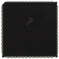
MC68HC711E9CFNE2 Freescale Semiconductor, MC68HC711E9CFNE2 Datasheet - Page 148

MC68HC711E9CFNE2
Manufacturer Part Number
MC68HC711E9CFNE2
Description
IC MCU 8BIT 512RAM 52-PLC
Manufacturer
Freescale Semiconductor
Series
HC11r
Datasheet
1.MC68HC711E9CFNE3.pdf
(336 pages)
Specifications of MC68HC711E9CFNE2
Core Processor
HC11
Core Size
8-Bit
Speed
2MHz
Connectivity
SCI, SPI
Peripherals
POR, WDT
Number Of I /o
38
Program Memory Size
12KB (12K x 8)
Program Memory Type
OTP
Eeprom Size
512 x 8
Ram Size
512 x 8
Voltage - Supply (vcc/vdd)
4.5 V ~ 5.5 V
Data Converters
A/D 8x8b
Oscillator Type
Internal
Operating Temperature
-40°C ~ 85°C
Package / Case
52-PLCC
Processor Series
HC711E
Core
HC11
Data Bus Width
8 bit
Data Ram Size
512 B
Interface Type
SCI, SPI
Maximum Clock Frequency
2 MHz
Number Of Programmable I/os
38
Number Of Timers
8
Maximum Operating Temperature
+ 85 C
Mounting Style
SMD/SMT
Minimum Operating Temperature
- 40 C
On-chip Adc
8 bit
Lead Free Status / RoHS Status
Lead free / RoHS Compliant
Available stocks
Company
Part Number
Manufacturer
Quantity
Price
Company:
Part Number:
MC68HC711E9CFNE2
Manufacturer:
TE
Quantity:
12 000
Company:
Part Number:
MC68HC711E9CFNE2
Manufacturer:
FREESCAL
Quantity:
5 530
- Current page: 148 of 336
- Download datasheet (4Mb)
Serial Communications Interface (SCI)
7.5 Receive Operation
7.6 Wakeup Feature
Technical Data
148
During receive operations, the transmit sequence is reversed. The serial
shift register receives data and transfers it to a parallel receive data
register (SCDR) as a complete word. This double buffered operation
allows a character to be shifted in serially while another character is
already in the SCDR. An advanced data recovery scheme distinguishes
valid data from noise in the serial data stream. The data input is
selectively sampled to detect receive data, and a majority voting circuit
determines the value and integrity of each bit. See
The wakeup feature reduces SCI service overhead in multiple receiver
systems. Software for each receiver evaluates the first character of each
message. The receiver is placed in wakeup mode by writing a 1 to the
RWU bit in the SCCR2 register. While RWU is 1, all of the
receiver-related status flags (RDRF, IDLE, OR, NF, and FE) are
inhibited (cannot become set). Although RWU can be cleared by a
software write to SCCR2, to do so would be unusual. Normally, RWU is
set by software and is cleared automatically with hardware. Whenever a
new message begins, logic alerts the sleeping receivers to wake up and
evaluate the initial character of the new message.
Two methods of wakeup are available:
During idle-line wakeup, a sleeping receiver awakens as soon as the
RxD line becomes idle. In the address-mark wakeup, logic 1 in the most
significant bit (MSB) of a character wakes up all sleeping receivers.
•
•
Idle-line wakeup
Address-mark wakeup
Serial Communications Interface (SCI)
M68HC11E Family — Rev. 3.2
Figure
7-2.
MOTOROLA
Related parts for MC68HC711E9CFNE2
Image
Part Number
Description
Manufacturer
Datasheet
Request
R

Part Number:
Description:
APPENDIX A ELECTRICAL CHARACTERISTICS
Manufacturer:
FREESCALE [Freescale Semiconductor, Inc]
Datasheet:
Part Number:
Description:
Manufacturer:
Freescale Semiconductor, Inc
Datasheet:
Part Number:
Description:
Manufacturer:
Freescale Semiconductor, Inc
Datasheet:
Part Number:
Description:
Manufacturer:
Freescale Semiconductor, Inc
Datasheet:
Part Number:
Description:
Manufacturer:
Freescale Semiconductor, Inc
Datasheet:
Part Number:
Description:
Manufacturer:
Freescale Semiconductor, Inc
Datasheet:
Part Number:
Description:
Manufacturer:
Freescale Semiconductor, Inc
Datasheet:
Part Number:
Description:
Manufacturer:
Freescale Semiconductor, Inc
Datasheet:
Part Number:
Description:
Manufacturer:
Freescale Semiconductor, Inc
Datasheet:
Part Number:
Description:
Manufacturer:
Freescale Semiconductor, Inc
Datasheet:
Part Number:
Description:
Manufacturer:
Freescale Semiconductor, Inc
Datasheet:
Part Number:
Description:
Manufacturer:
Freescale Semiconductor, Inc
Datasheet:
Part Number:
Description:
Manufacturer:
Freescale Semiconductor, Inc
Datasheet:
Part Number:
Description:
Manufacturer:
Freescale Semiconductor, Inc
Datasheet:
Part Number:
Description:
Manufacturer:
Freescale Semiconductor, Inc
Datasheet:


