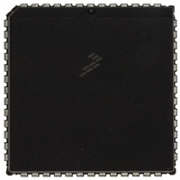
MC68HC711E9CFNE2 Freescale Semiconductor, MC68HC711E9CFNE2 Datasheet - Page 182

MC68HC711E9CFNE2
Manufacturer Part Number
MC68HC711E9CFNE2
Description
IC MCU 8BIT 512RAM 52-PLC
Manufacturer
Freescale Semiconductor
Series
HC11r
Datasheet
1.MC68HC711E9CFNE3.pdf
(336 pages)
Specifications of MC68HC711E9CFNE2
Core Processor
HC11
Core Size
8-Bit
Speed
2MHz
Connectivity
SCI, SPI
Peripherals
POR, WDT
Number Of I /o
38
Program Memory Size
12KB (12K x 8)
Program Memory Type
OTP
Eeprom Size
512 x 8
Ram Size
512 x 8
Voltage - Supply (vcc/vdd)
4.5 V ~ 5.5 V
Data Converters
A/D 8x8b
Oscillator Type
Internal
Operating Temperature
-40°C ~ 85°C
Package / Case
52-PLCC
Processor Series
HC711E
Core
HC11
Data Bus Width
8 bit
Data Ram Size
512 B
Interface Type
SCI, SPI
Maximum Clock Frequency
2 MHz
Number Of Programmable I/os
38
Number Of Timers
8
Maximum Operating Temperature
+ 85 C
Mounting Style
SMD/SMT
Minimum Operating Temperature
- 40 C
On-chip Adc
8 bit
Lead Free Status / RoHS Status
Lead free / RoHS Compliant
Available stocks
Company
Part Number
Manufacturer
Quantity
Price
Company:
Part Number:
MC68HC711E9CFNE2
Manufacturer:
TE
Quantity:
12 000
Company:
Part Number:
MC68HC711E9CFNE2
Manufacturer:
FREESCAL
Quantity:
5 530
- Current page: 182 of 336
- Download datasheet (4Mb)
Timing System
9.4 Input Capture
Technical Data
182
The input capture function records the time an external event occurs by
latching the value of the free-running counter when a selected edge is
detected at the associated timer input pin. Software can store latched
values and use them to compute the periodicity and duration of events.
For example, by storing the times of successive edges of an incoming
signal, software can determine the period and pulse width of a signal. To
measure period, two successive edges of the same polarity are
captured. To measure pulse width, two alternate polarity edges are
captured.
In most cases, input capture edges are asynchronous to the internal
timer counter, which is clocked relative to an internal clock (PH2). These
asynchronous capture requests are synchronized to PH2 so that the
latching occurs on the opposite half cycle of PH2 from when the timer
counter is being incremented. This synchronization process introduces
a delay from when the edge occurs to when the counter value is
detected. Because these delays offset each other when the time
between two edges is being measured, the delay can be ignored. When
an input capture is being used with an output compare, there is a similar
delay between the actual compare point and when the output pin
changes state.
The control and status bits that implement the input capture functions
are contained in:
To configure port A bit 3 as an input capture, clear the DDRA3 bit of the
PACTL register. Note that this bit is cleared out of reset. To enable PA3
as the fourth input capture, set the I4/O5 bit in the PACTL register.
Otherwise, PA3 is configured as a fifth output compare out of reset, with
bit I4/O5 being cleared. If the DDRA3 bit is set (configuring PA3 as an
output), and IC4 is enabled, then writes to PA3 cause edges on the pin
•
•
•
•
Pulse accumulator control register (PACTL)
Timer control 2 register (TCTL2)
Timer interrupt mask 1 register (TMSK1)
Timer interrupt flag 2 register (TFLG1)
Timing System
M68HC11E Family — Rev. 3.2
MOTOROLA
Related parts for MC68HC711E9CFNE2
Image
Part Number
Description
Manufacturer
Datasheet
Request
R

Part Number:
Description:
APPENDIX A ELECTRICAL CHARACTERISTICS
Manufacturer:
FREESCALE [Freescale Semiconductor, Inc]
Datasheet:
Part Number:
Description:
Manufacturer:
Freescale Semiconductor, Inc
Datasheet:
Part Number:
Description:
Manufacturer:
Freescale Semiconductor, Inc
Datasheet:
Part Number:
Description:
Manufacturer:
Freescale Semiconductor, Inc
Datasheet:
Part Number:
Description:
Manufacturer:
Freescale Semiconductor, Inc
Datasheet:
Part Number:
Description:
Manufacturer:
Freescale Semiconductor, Inc
Datasheet:
Part Number:
Description:
Manufacturer:
Freescale Semiconductor, Inc
Datasheet:
Part Number:
Description:
Manufacturer:
Freescale Semiconductor, Inc
Datasheet:
Part Number:
Description:
Manufacturer:
Freescale Semiconductor, Inc
Datasheet:
Part Number:
Description:
Manufacturer:
Freescale Semiconductor, Inc
Datasheet:
Part Number:
Description:
Manufacturer:
Freescale Semiconductor, Inc
Datasheet:
Part Number:
Description:
Manufacturer:
Freescale Semiconductor, Inc
Datasheet:
Part Number:
Description:
Manufacturer:
Freescale Semiconductor, Inc
Datasheet:
Part Number:
Description:
Manufacturer:
Freescale Semiconductor, Inc
Datasheet:
Part Number:
Description:
Manufacturer:
Freescale Semiconductor, Inc
Datasheet:


