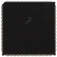
MC68HC711E9CFNE2 Freescale Semiconductor, MC68HC711E9CFNE2 Datasheet - Page 186

MC68HC711E9CFNE2
Manufacturer Part Number
MC68HC711E9CFNE2
Description
IC MCU 8BIT 512RAM 52-PLC
Manufacturer
Freescale Semiconductor
Series
HC11r
Datasheet
1.MC68HC711E9CFNE3.pdf
(336 pages)
Specifications of MC68HC711E9CFNE2
Core Processor
HC11
Core Size
8-Bit
Speed
2MHz
Connectivity
SCI, SPI
Peripherals
POR, WDT
Number Of I /o
38
Program Memory Size
12KB (12K x 8)
Program Memory Type
OTP
Eeprom Size
512 x 8
Ram Size
512 x 8
Voltage - Supply (vcc/vdd)
4.5 V ~ 5.5 V
Data Converters
A/D 8x8b
Oscillator Type
Internal
Operating Temperature
-40°C ~ 85°C
Package / Case
52-PLCC
Processor Series
HC711E
Core
HC11
Data Bus Width
8 bit
Data Ram Size
512 B
Interface Type
SCI, SPI
Maximum Clock Frequency
2 MHz
Number Of Programmable I/os
38
Number Of Timers
8
Maximum Operating Temperature
+ 85 C
Mounting Style
SMD/SMT
Minimum Operating Temperature
- 40 C
On-chip Adc
8 bit
Lead Free Status / RoHS Status
Lead free / RoHS Compliant
Available stocks
Company
Part Number
Manufacturer
Quantity
Price
Company:
Part Number:
MC68HC711E9CFNE2
Manufacturer:
TE
Quantity:
12 000
Company:
Part Number:
MC68HC711E9CFNE2
Manufacturer:
FREESCAL
Quantity:
5 530
- Current page: 186 of 336
- Download datasheet (4Mb)
Timing System
9.4.3 Timer Input Capture 4/Output Compare 5 Register
9.5 Output Compare
Technical Data
186
Register name: Timer Input Capture 4/Output Compare 5 (High)
Register name: Timer Input Capture 4/Output Compare 5 (Low)
Use TI4/O5 as either an input capture register or an output compare
register, depending on the function chosen for the PA3 pin. To enable it
as an input capture pin, set the I4/O5 bit in the pulse accumulator control
register (PACTL) to logic level 1. To use it as an output compare register,
set the I4/O5 bit to a logic level 0. Refer to
Use the output compare (OC) function to program an action to occur at
a specific time — when the 16-bit counter reaches a specified value. For
each of the five output compare functions, there is a separate 16-bit
compare register and a dedicated 16-bit comparator. The value in the
compare register is compared to the value of the free-running counter on
every bus cycle. When the compare register matches the counter value,
an output compare status flag is set. The flag can be used to initiate the
automatic actions for that output compare function.
To produce a pulse of a specific duration, write a value to the output
compare register that represents the time the leading edge of the pulse
is to occur. The output compare circuit is configured to set the
Reset:
Reset:
Read:
Read:
Write:
Write:
Bit 15
Bit 7
Bit 7
Bit 7
1
1
Figure 9-7. Timer Input Capture 4/Output
Bit 14
Bit 6
Compare 5 Register Pair (TI4/O5)
Timing System
6
1
6
1
Bit 13
Bit 5
5
1
5
1
Bit 12
Bit 4
4
1
4
1
Bit 11
Bit 3
3
1
3
1
9.8 Pulse
Address: $101F
Address: $101E
M68HC11E Family — Rev. 3.2
Bit 10
Bit 2
2
1
2
1
Accumulator.
Bit 9
Bit 1
1
1
1
1
MOTOROLA
Bit 0
Bit 8
Bit 0
Bit 0
1
1
Related parts for MC68HC711E9CFNE2
Image
Part Number
Description
Manufacturer
Datasheet
Request
R

Part Number:
Description:
APPENDIX A ELECTRICAL CHARACTERISTICS
Manufacturer:
FREESCALE [Freescale Semiconductor, Inc]
Datasheet:
Part Number:
Description:
Manufacturer:
Freescale Semiconductor, Inc
Datasheet:
Part Number:
Description:
Manufacturer:
Freescale Semiconductor, Inc
Datasheet:
Part Number:
Description:
Manufacturer:
Freescale Semiconductor, Inc
Datasheet:
Part Number:
Description:
Manufacturer:
Freescale Semiconductor, Inc
Datasheet:
Part Number:
Description:
Manufacturer:
Freescale Semiconductor, Inc
Datasheet:
Part Number:
Description:
Manufacturer:
Freescale Semiconductor, Inc
Datasheet:
Part Number:
Description:
Manufacturer:
Freescale Semiconductor, Inc
Datasheet:
Part Number:
Description:
Manufacturer:
Freescale Semiconductor, Inc
Datasheet:
Part Number:
Description:
Manufacturer:
Freescale Semiconductor, Inc
Datasheet:
Part Number:
Description:
Manufacturer:
Freescale Semiconductor, Inc
Datasheet:
Part Number:
Description:
Manufacturer:
Freescale Semiconductor, Inc
Datasheet:
Part Number:
Description:
Manufacturer:
Freescale Semiconductor, Inc
Datasheet:
Part Number:
Description:
Manufacturer:
Freescale Semiconductor, Inc
Datasheet:
Part Number:
Description:
Manufacturer:
Freescale Semiconductor, Inc
Datasheet:


