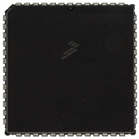
MC68HC711E9CFNE2 Freescale Semiconductor, MC68HC711E9CFNE2 Datasheet - Page 214

MC68HC711E9CFNE2
Manufacturer Part Number
MC68HC711E9CFNE2
Description
IC MCU 8BIT 512RAM 52-PLC
Manufacturer
Freescale Semiconductor
Series
HC11r
Datasheet
1.MC68HC711E9CFNE3.pdf
(336 pages)
Specifications of MC68HC711E9CFNE2
Core Processor
HC11
Core Size
8-Bit
Speed
2MHz
Connectivity
SCI, SPI
Peripherals
POR, WDT
Number Of I /o
38
Program Memory Size
12KB (12K x 8)
Program Memory Type
OTP
Eeprom Size
512 x 8
Ram Size
512 x 8
Voltage - Supply (vcc/vdd)
4.5 V ~ 5.5 V
Data Converters
A/D 8x8b
Oscillator Type
Internal
Operating Temperature
-40°C ~ 85°C
Package / Case
52-PLCC
Processor Series
HC711E
Core
HC11
Data Bus Width
8 bit
Data Ram Size
512 B
Interface Type
SCI, SPI
Maximum Clock Frequency
2 MHz
Number Of Programmable I/os
38
Number Of Timers
8
Maximum Operating Temperature
+ 85 C
Mounting Style
SMD/SMT
Minimum Operating Temperature
- 40 C
On-chip Adc
8 bit
Lead Free Status / RoHS Status
Lead free / RoHS Compliant
Available stocks
Company
Part Number
Manufacturer
Quantity
Price
Company:
Part Number:
MC68HC711E9CFNE2
Manufacturer:
TE
Quantity:
12 000
Company:
Part Number:
MC68HC711E9CFNE2
Manufacturer:
FREESCAL
Quantity:
5 530
- Current page: 214 of 336
- Download datasheet (4Mb)
Analog-to-Digital (A/D) Converter
10.4 A/D Converter Power-Up and Clock Select
Technical Data
214
1. Can be written only once in first 64 cycles out of reset in normal modes or at any time in special modes
Address:
Bit 7 of the OPTION register controls A/D converter power-up. Clearing
ADPU removes power from and disables the A/D converter system.
Setting ADPU enables the A/D converter system. Stabilization of the
analog bias voltages requires a delay of as much as 100 s after turning
on the A/D converter. When the A/D converter system is operating with
the MCU E clock, all switching and comparator operations are inherently
synchronized to the main MCU clocks. This allows the comparator
output to be sampled at relatively quiet times during MCU clock cycles.
Since the internal RC oscillator is asynchronous to the MCU clock, there
is more error attributable to internal system clock noise. A/D converter
accuracy is reduced slightly while the internal RC oscillator is being used
(CSEL = 1).
ADPU — A/D Power-Up Bit
CSEL — Clock Select Bit
IRQE — Configure IRQ for Edge-Sensitive Only Operation
Reset:
Read:
Figure 10-4. System Configuration Options Register (OPTION)
Write:
Refer to
0 = A/D powered down
1 = A/D powered up
0 = A/D and EEPROM use system E clock.
1 = A/D and EEPROM use internal RC clock.
$1039
ADPU
Bit 7
0
Analog-to-Digital (A/D) Converter
Section 5. Resets and
= Unimplemented
CSEL
6
0
IRQE
5
0
(1)
DLY
4
1
(1)
Interrupts.
CME
3
0
M68HC11E Family — Rev. 3.2
2
0
CR1
1
0
(1)
MOTOROLA
CR0
Bit 0
0
(1)
Related parts for MC68HC711E9CFNE2
Image
Part Number
Description
Manufacturer
Datasheet
Request
R

Part Number:
Description:
APPENDIX A ELECTRICAL CHARACTERISTICS
Manufacturer:
FREESCALE [Freescale Semiconductor, Inc]
Datasheet:
Part Number:
Description:
Manufacturer:
Freescale Semiconductor, Inc
Datasheet:
Part Number:
Description:
Manufacturer:
Freescale Semiconductor, Inc
Datasheet:
Part Number:
Description:
Manufacturer:
Freescale Semiconductor, Inc
Datasheet:
Part Number:
Description:
Manufacturer:
Freescale Semiconductor, Inc
Datasheet:
Part Number:
Description:
Manufacturer:
Freescale Semiconductor, Inc
Datasheet:
Part Number:
Description:
Manufacturer:
Freescale Semiconductor, Inc
Datasheet:
Part Number:
Description:
Manufacturer:
Freescale Semiconductor, Inc
Datasheet:
Part Number:
Description:
Manufacturer:
Freescale Semiconductor, Inc
Datasheet:
Part Number:
Description:
Manufacturer:
Freescale Semiconductor, Inc
Datasheet:
Part Number:
Description:
Manufacturer:
Freescale Semiconductor, Inc
Datasheet:
Part Number:
Description:
Manufacturer:
Freescale Semiconductor, Inc
Datasheet:
Part Number:
Description:
Manufacturer:
Freescale Semiconductor, Inc
Datasheet:
Part Number:
Description:
Manufacturer:
Freescale Semiconductor, Inc
Datasheet:
Part Number:
Description:
Manufacturer:
Freescale Semiconductor, Inc
Datasheet:


