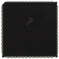
MC68HC711E9CFNE2 Freescale Semiconductor, MC68HC711E9CFNE2 Datasheet - Page 240

MC68HC711E9CFNE2
Manufacturer Part Number
MC68HC711E9CFNE2
Description
IC MCU 8BIT 512RAM 52-PLC
Manufacturer
Freescale Semiconductor
Series
HC11r
Datasheet
1.MC68HC711E9CFNE3.pdf
(336 pages)
Specifications of MC68HC711E9CFNE2
Core Processor
HC11
Core Size
8-Bit
Speed
2MHz
Connectivity
SCI, SPI
Peripherals
POR, WDT
Number Of I /o
38
Program Memory Size
12KB (12K x 8)
Program Memory Type
OTP
Eeprom Size
512 x 8
Ram Size
512 x 8
Voltage - Supply (vcc/vdd)
4.5 V ~ 5.5 V
Data Converters
A/D 8x8b
Oscillator Type
Internal
Operating Temperature
-40°C ~ 85°C
Package / Case
52-PLCC
Processor Series
HC711E
Core
HC11
Data Bus Width
8 bit
Data Ram Size
512 B
Interface Type
SCI, SPI
Maximum Clock Frequency
2 MHz
Number Of Programmable I/os
38
Number Of Timers
8
Maximum Operating Temperature
+ 85 C
Mounting Style
SMD/SMT
Minimum Operating Temperature
- 40 C
On-chip Adc
8 bit
Lead Free Status / RoHS Status
Lead free / RoHS Compliant
Available stocks
Company
Part Number
Manufacturer
Quantity
Price
Company:
Part Number:
MC68HC711E9CFNE2
Manufacturer:
TE
Quantity:
12 000
Company:
Part Number:
MC68HC711E9CFNE2
Manufacturer:
FREESCAL
Quantity:
5 530
- Current page: 240 of 336
- Download datasheet (4Mb)
Electrical Characteristics
11.14 Analog-to-Digital Converter Characteristics
Technical Data
240
Resolution
Non-linearity
Zero error
Full scale error
Total unadjusted
Quantization
Absolute
Conversion
V
V
Conversion
Monotonicity
Zero input
Full scale
Sample
Sample/hold
Input leakage
Characteristic
1. V
2. Source impedances greater than 10 k affect accuracy adversely because of input leakage.
3. Performance verified down to 2.5 V V
V
RH
RL
error
error
accuracy
range
time
reading
acquisition
time
capacitance
reading
R
DD
= 5.0 Vdc 10%, V
(1)
Number of bits resolved by A/D converter
Maximum deviation from the ideal A/D
Difference between the output of an ideal and
Difference between the output of an ideal and
Maximum sum of non-linearity, zero error, and
Uncertainty because of converter resolution
Difference between the actual input voltage
Analog input voltage range
Maximum analog reference voltage
Minimum analog reference voltage
Minimum difference between V
Total time to perform a single A/D conversion:
Conversion result never decreases with an
Conversion result when V
Conversion result when V
Analog input acquisition sampling time:
Input capacitance during sample
Input leakage on A/D pins
transfer characteristics
an actual for 0 input voltage
an actual A/D for full-scale input voltage
full-scale error
and the full-scale weighted equivalent of the
binary output code, all error sources
included
E clock
Internal RC oscillator
increase in input voltage; has no missing
codes
E clock
Internal RC oscillator
PE[7:0]
PE[7:0]
V
RL
, V
SS
RH
= 0 Vdc, T
Parameter
A
= T
R
, but accuracy is tested and guaranteed at V
L
to T
Electrical Characteristics
In
In
(2)
H,
= V
= V
750 kHz
RH
RL
RH
and V
(2)
(3)
E
RL
(2)
3.0 MHz, unless otherwise noted
V
SS
Min
V
V
00
—
—
—
—
—
—
—
—
—
—
—
—
—
—
—
—
3
RL
RL
–0.1
Guaranteed
Absolute
20 typical
32
12
—
—
—
—
—
—
—
—
—
—
—
—
—
—
—
—
8
R
= 5 V 10%.
M68HC11E Family — Rev. 3.2
V
2.0 MHz 3.0 MHz
t
cyc
DD
Max
V
V
400
1.0
FF
12
—
—
—
—
—
—
—
1/2
1/2
1/2
1/2
1/2
RH
RH
1
+0.1 V
+32
t
cyc
DD
MOTOROLA
Max
V
V
400
1.0
FF
—
—
—
—
—
—
12
—
1/2
1/2
RH
RH
1
1
1
2
+0.1
+32
Unit
LSB
LSB
LSB
LSB
LSB
LSB
Hex
Hex
Bits
t
t
nA
pF
—
cyc
cyc
V
V
V
V
A
s
s
Related parts for MC68HC711E9CFNE2
Image
Part Number
Description
Manufacturer
Datasheet
Request
R

Part Number:
Description:
APPENDIX A ELECTRICAL CHARACTERISTICS
Manufacturer:
FREESCALE [Freescale Semiconductor, Inc]
Datasheet:
Part Number:
Description:
Manufacturer:
Freescale Semiconductor, Inc
Datasheet:
Part Number:
Description:
Manufacturer:
Freescale Semiconductor, Inc
Datasheet:
Part Number:
Description:
Manufacturer:
Freescale Semiconductor, Inc
Datasheet:
Part Number:
Description:
Manufacturer:
Freescale Semiconductor, Inc
Datasheet:
Part Number:
Description:
Manufacturer:
Freescale Semiconductor, Inc
Datasheet:
Part Number:
Description:
Manufacturer:
Freescale Semiconductor, Inc
Datasheet:
Part Number:
Description:
Manufacturer:
Freescale Semiconductor, Inc
Datasheet:
Part Number:
Description:
Manufacturer:
Freescale Semiconductor, Inc
Datasheet:
Part Number:
Description:
Manufacturer:
Freescale Semiconductor, Inc
Datasheet:
Part Number:
Description:
Manufacturer:
Freescale Semiconductor, Inc
Datasheet:
Part Number:
Description:
Manufacturer:
Freescale Semiconductor, Inc
Datasheet:
Part Number:
Description:
Manufacturer:
Freescale Semiconductor, Inc
Datasheet:
Part Number:
Description:
Manufacturer:
Freescale Semiconductor, Inc
Datasheet:
Part Number:
Description:
Manufacturer:
Freescale Semiconductor, Inc
Datasheet:


