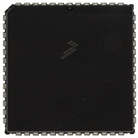
MC68HC711E9CFNE2 Freescale Semiconductor, MC68HC711E9CFNE2 Datasheet - Page 48

MC68HC711E9CFNE2
Manufacturer Part Number
MC68HC711E9CFNE2
Description
IC MCU 8BIT 512RAM 52-PLC
Manufacturer
Freescale Semiconductor
Series
HC11r
Datasheet
1.MC68HC711E9CFNE3.pdf
(336 pages)
Specifications of MC68HC711E9CFNE2
Core Processor
HC11
Core Size
8-Bit
Speed
2MHz
Connectivity
SCI, SPI
Peripherals
POR, WDT
Number Of I /o
38
Program Memory Size
12KB (12K x 8)
Program Memory Type
OTP
Eeprom Size
512 x 8
Ram Size
512 x 8
Voltage - Supply (vcc/vdd)
4.5 V ~ 5.5 V
Data Converters
A/D 8x8b
Oscillator Type
Internal
Operating Temperature
-40°C ~ 85°C
Package / Case
52-PLCC
Processor Series
HC711E
Core
HC11
Data Bus Width
8 bit
Data Ram Size
512 B
Interface Type
SCI, SPI
Maximum Clock Frequency
2 MHz
Number Of Programmable I/os
38
Number Of Timers
8
Maximum Operating Temperature
+ 85 C
Mounting Style
SMD/SMT
Minimum Operating Temperature
- 40 C
On-chip Adc
8 bit
Lead Free Status / RoHS Status
Lead free / RoHS Compliant
Available stocks
Company
Part Number
Manufacturer
Quantity
Price
Company:
Part Number:
MC68HC711E9CFNE2
Manufacturer:
TE
Quantity:
12 000
Company:
Part Number:
MC68HC711E9CFNE2
Manufacturer:
FREESCAL
Quantity:
5 530
- Current page: 48 of 336
- Download datasheet (4Mb)
Central Processor Unit (CPU)
3.3.2 Index Register X (IX)
3.3.3 Index Register Y (IY)
3.3.4 Stack Pointer (SP)
Technical Data
48
The IX register provides a 16-bit indexing value that can be added to the
8-bit offset provided in an instruction to create an effective address. The
IX register can also be used as a counter or as a temporary storage
register.
The 16-bit IY register performs an indexed mode function similar to that
of the IX register. However, most instructions using the IY register
require an extra byte of machine code and an extra cycle of execution
time because of the way the opcode map is implemented. Refer to
3.5 Opcodes and Operands
The M68HC11 CPU has an automatic program stack. This stack can be
located anywhere in the address space and can be any size up to the
amount of memory available in the system. Normally, the SP is initialized
by one of the first instructions in an application program. The stack is
configured as a data structure that grows downward from high memory
to low memory. Each time a new byte is pushed onto the stack, the SP
is decremented. Each time a byte is pulled from the stack, the SP is
incremented. At any given time, the SP holds the 16-bit address of the
next free location in the stack.
operations.
•
•
The decimal adjust accumulator A (DAA) instruction is used after
binary-coded decimal (BCD) arithmetic operations, but there is no
equivalent BCD instruction to adjust accumulator B.
The add, subtract, and compare instructions associated with both
A and B (ABA, SBA, and CBA) only operate in one direction,
making it important to plan ahead to ensure that the correct
operand is in the correct accumulator.
Central Processor Unit (CPU)
for further information.
Figure 3-2
is a summary of SP
M68HC11E Family — Rev. 3.2
MOTOROLA
Related parts for MC68HC711E9CFNE2
Image
Part Number
Description
Manufacturer
Datasheet
Request
R

Part Number:
Description:
APPENDIX A ELECTRICAL CHARACTERISTICS
Manufacturer:
FREESCALE [Freescale Semiconductor, Inc]
Datasheet:
Part Number:
Description:
Manufacturer:
Freescale Semiconductor, Inc
Datasheet:
Part Number:
Description:
Manufacturer:
Freescale Semiconductor, Inc
Datasheet:
Part Number:
Description:
Manufacturer:
Freescale Semiconductor, Inc
Datasheet:
Part Number:
Description:
Manufacturer:
Freescale Semiconductor, Inc
Datasheet:
Part Number:
Description:
Manufacturer:
Freescale Semiconductor, Inc
Datasheet:
Part Number:
Description:
Manufacturer:
Freescale Semiconductor, Inc
Datasheet:
Part Number:
Description:
Manufacturer:
Freescale Semiconductor, Inc
Datasheet:
Part Number:
Description:
Manufacturer:
Freescale Semiconductor, Inc
Datasheet:
Part Number:
Description:
Manufacturer:
Freescale Semiconductor, Inc
Datasheet:
Part Number:
Description:
Manufacturer:
Freescale Semiconductor, Inc
Datasheet:
Part Number:
Description:
Manufacturer:
Freescale Semiconductor, Inc
Datasheet:
Part Number:
Description:
Manufacturer:
Freescale Semiconductor, Inc
Datasheet:
Part Number:
Description:
Manufacturer:
Freescale Semiconductor, Inc
Datasheet:
Part Number:
Description:
Manufacturer:
Freescale Semiconductor, Inc
Datasheet:


