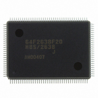
HD64F2638F20J Renesas Electronics America, HD64F2638F20J Datasheet - Page 107

HD64F2638F20J
Manufacturer Part Number
HD64F2638F20J
Description
IC H8S MCU FLASH 256K 128-QFP
Manufacturer
Renesas Electronics America
Series
H8® H8S/2600r
Specifications of HD64F2638F20J
Core Processor
H8S/2600
Core Size
16-Bit
Speed
20MHz
Connectivity
CAN, SCI, SmartCard
Peripherals
Motor Control PWM, POR, PWM, WDT
Number Of I /o
72
Program Memory Size
256KB (256K x 8)
Program Memory Type
FLASH
Ram Size
16K x 8
Voltage - Supply (vcc/vdd)
4.5 V ~ 5.5 V
Data Converters
A/D 12x10b; D/A 2x8b
Oscillator Type
Internal
Operating Temperature
-40°C ~ 85°C
Package / Case
128-QFP
Lead Free Status / RoHS Status
Contains lead / RoHS non-compliant
Eeprom Size
-
Available stocks
Company
Part Number
Manufacturer
Quantity
Price
Company:
Part Number:
HD64F2638F20J
Manufacturer:
PENESAS
Quantity:
252
- Current page: 107 of 1512
- Download datasheet (9Mb)
H8S/2639, H8S/2638, H8S/2636,
H8S/2630, H8S/2635 Group
(4) Register Indirect with Post-Increment or Pre-Decrement—@ERn+ or @-ERn:
• Register indirect with post-increment—@ERn+
• Register indirect with pre-decrement—@-ERn
(5) Absolute Address—@aa:8, @aa:16, @aa:24, or @aa:32: The instruction code contains the
absolute address of a memory operand. The absolute address may be 8 bits long (@aa:8), 16 bits
long (@aa:16), 24 bits long (@aa:24), or 32 bits long (@aa:32).
To access data, the absolute address should be 8 bits (@aa:8), 16 bits (@aa:16), or 32 bits
(@aa:32) long. For an 8-bit absolute address, the upper 24 bits are all assumed to be 1 (H'FFFF).
For a 16-bit absolute address the upper 16 bits are a sign extension. A 32-bit absolute address can
access the entire address space.
A 24-bit absolute address (@aa:24) indicates the address of a program instruction. The upper 8
bits are all assumed to be 0 (H'00).
Table 2-5 indicates the accessible absolute address ranges.
Table 2-5
Absolute Address
Data address
Program instruction
address
Note: * Not available in the chip.
REJ09B0103-0800 Rev. 8.00
May 28, 2010
The register field of the instruction code specifies an address register (ERn) which contains the
address of a memory operand. After the operand is accessed, 1, 2, or 4 is added to the address
register contents and the sum is stored in the address register. The value added is 1 for byte
access, 2 for word transfer instruction, or 4 for longword transfer instruction. For word or
longword transfer instruction, the register value should be even.
The value 1, 2, or 4 is subtracted from an address register (ERn) specified by the register field
in the instruction code, and the result becomes the address of a memory operand. The result is
also stored in the address register. The value subtracted is 1 for byte access, 2 for word transfer
instruction, or 4 for longword transfer instruction. For word or longword transfer instruction,
the register value should be even.
Absolute Address Access Ranges
8 bits (@aa:8)
16 bits (@aa:16)
32 bits (@aa:32)
24 bits (@aa:24)
Normal Mode *
H'FF00 to H'FFFF
H'0000 to H'FFFF
H'FFFF00 to H'FFFFFF
Advanced Mode
H'000000 to H'007FFF,
H'FF8000 to H'FFFFFF
H'000000 to H'FFFFFF
Page 57 of 1458
Section 2 CPU
Related parts for HD64F2638F20J
Image
Part Number
Description
Manufacturer
Datasheet
Request
R

Part Number:
Description:
KIT STARTER FOR M16C/29
Manufacturer:
Renesas Electronics America
Datasheet:

Part Number:
Description:
KIT STARTER FOR R8C/2D
Manufacturer:
Renesas Electronics America
Datasheet:

Part Number:
Description:
R0K33062P STARTER KIT
Manufacturer:
Renesas Electronics America
Datasheet:

Part Number:
Description:
KIT STARTER FOR R8C/23 E8A
Manufacturer:
Renesas Electronics America
Datasheet:

Part Number:
Description:
KIT STARTER FOR R8C/25
Manufacturer:
Renesas Electronics America
Datasheet:

Part Number:
Description:
KIT STARTER H8S2456 SHARPE DSPLY
Manufacturer:
Renesas Electronics America
Datasheet:

Part Number:
Description:
KIT STARTER FOR R8C38C
Manufacturer:
Renesas Electronics America
Datasheet:

Part Number:
Description:
KIT STARTER FOR R8C35C
Manufacturer:
Renesas Electronics America
Datasheet:

Part Number:
Description:
KIT STARTER FOR R8CL3AC+LCD APPS
Manufacturer:
Renesas Electronics America
Datasheet:

Part Number:
Description:
KIT STARTER FOR RX610
Manufacturer:
Renesas Electronics America
Datasheet:

Part Number:
Description:
KIT STARTER FOR R32C/118
Manufacturer:
Renesas Electronics America
Datasheet:

Part Number:
Description:
KIT DEV RSK-R8C/26-29
Manufacturer:
Renesas Electronics America
Datasheet:

Part Number:
Description:
KIT STARTER FOR SH7124
Manufacturer:
Renesas Electronics America
Datasheet:

Part Number:
Description:
KIT STARTER FOR H8SX/1622
Manufacturer:
Renesas Electronics America
Datasheet:


