HD64F2638F20J Renesas Electronics America, HD64F2638F20J Datasheet - Page 43
HD64F2638F20J
Manufacturer Part Number
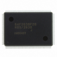
HD64F2638F20J
Description
IC H8S MCU FLASH 256K 128-QFP
Manufacturer
Renesas Electronics America
Series
H8® H8S/2600r
Specifications of HD64F2638F20J
Core Processor
H8S/2600
Core Size
16-Bit
Speed
20MHz
Connectivity
CAN, SCI, SmartCard
Peripherals
Motor Control PWM, POR, PWM, WDT
Number Of I /o
72
Program Memory Size
256KB (256K x 8)
Program Memory Type
FLASH
Ram Size
16K x 8
Voltage - Supply (vcc/vdd)
4.5 V ~ 5.5 V
Data Converters
A/D 12x10b; D/A 2x8b
Oscillator Type
Internal
Operating Temperature
-40°C ~ 85°C
Package / Case
128-QFP
Lead Free Status / RoHS Status
Contains lead / RoHS non-compliant
Eeprom Size
-
Available stocks
Company
Part Number
Manufacturer
Quantity
Price
Company:

Part Number:
HD64F2638F20J
Manufacturer:
PENESAS
Quantity:
252


21A.9
21A.10 Protection ...................................................................................................................... 781
21A.11 Flash Memory Emulation in RAM................................................................................ 784
21A.12 Interrupt Handling when Programming/Erasing Flash Memory ................................... 786
21A.13 Programmer Mode......................................................................................................... 787
21A.14 Flash Memory and Power-Down States ........................................................................ 788
21A.15 Flash Memory Programming and Erasing Precautions ................................................. 789
21A.16 Note on Switching from F-ZTAT Version to Mask ROM Version............................... 794
Section 21B ROM (H8S/2638 Group, H8S/2639 Group, H8S/2630 Group)
21B.1
21B.2
21B.3
21B.4
21B.5
21B.6
21B.7
REJ09B0103-0800 Rev. 8.00
May 28, 2010
21A.8.1 Boot Mode .................................................................................................... 765
21A.8.2 User Program Mode...................................................................................... 769
Flash Memory Programming/Erasing ........................................................................... 771
21A.9.1 Program Mode .............................................................................................. 773
21A.9.2 Program-Verify Mode .................................................................................. 774
21A.9.3 Erase Mode ................................................................................................... 778
21A.9.4 Erase-Verify Mode ....................................................................................... 779
21A.10.1 Hardware Protection ..................................................................................... 781
21A.10.2 Software Protection ...................................................................................... 782
21A.10.3 Error Protection ............................................................................................ 782
21A.13.1 Socket Adapter and Memory Map................................................................ 787
21A.14.1 Notes on Power-Down States ....................................................................... 788
Overview ....................................................................................................................... 795
21B.1.1 Block Diagram.............................................................................................. 795
21B.1.2 Register Configuration.................................................................................. 796
Register Descriptions .................................................................................................... 796
21B.2.1 Mode Control Register (MDCR) .................................................................. 796
Operation....................................................................................................................... 796
Flash Memory Overview............................................................................................... 799
21B.4.1 Features......................................................................................................... 799
21B.4.2 Block Diagram.............................................................................................. 800
21B.4.3 Mode Transitions .......................................................................................... 801
21B.4.4 On-Board Programming Modes.................................................................... 802
21B.4.5 Flash Memory Emulation in RAM ............................................................... 804
21B.4.6 Differences between Boot Mode and User Program Mode .......................... 805
21B.4.7 Block Configuration ..................................................................................... 806
Pin Configuration .......................................................................................................... 807
Register Configuration .................................................................................................. 808
Register Descriptions .................................................................................................... 809
21B.7.1 Flash Memory Control Register 1 (FLMCR1) ............................................. 809
21B.7.2 Flash Memory Control Register 2 (FLMCR2) ............................................. 812
Page xliii of l
.... 795
Related parts for HD64F2638F20J
Image
Part Number
Description
Manufacturer
Datasheet
Request
R


Part Number:
Description:
KIT STARTER FOR M16C/29
Manufacturer:
Renesas Electronics America
Datasheet:

Part Number:
Description:
KIT STARTER FOR R8C/2D
Manufacturer:
Renesas Electronics America
Datasheet:

Part Number:
Description:
R0K33062P STARTER KIT
Manufacturer:
Renesas Electronics America
Datasheet:

Part Number:
Description:
KIT STARTER FOR R8C/23 E8A
Manufacturer:
Renesas Electronics America
Datasheet:

Part Number:
Description:
KIT STARTER FOR R8C/25
Manufacturer:
Renesas Electronics America
Datasheet:

Part Number:
Description:
KIT STARTER H8S2456 SHARPE DSPLY
Manufacturer:
Renesas Electronics America
Datasheet:

Part Number:
Description:
KIT STARTER FOR R8C38C
Manufacturer:
Renesas Electronics America
Datasheet:

Part Number:
Description:
KIT STARTER FOR R8C35C
Manufacturer:
Renesas Electronics America
Datasheet:

Part Number:
Description:
KIT STARTER FOR R8CL3AC+LCD APPS
Manufacturer:
Renesas Electronics America
Datasheet:
Part Number:
Description:
KIT STARTER FOR RX610
Manufacturer:
Renesas Electronics America
Datasheet:

Part Number:
Description:
KIT STARTER FOR R32C/118
Manufacturer:
Renesas Electronics America
Datasheet:

Part Number:
Description:
KIT DEV RSK-R8C/26-29
Manufacturer:
Renesas Electronics America
Datasheet:

Part Number:
Description:
KIT STARTER FOR SH7124
Manufacturer:
Renesas Electronics America
Datasheet:

Part Number:
Description:
KIT STARTER FOR H8SX/1622
Manufacturer:
Renesas Electronics America
Datasheet: